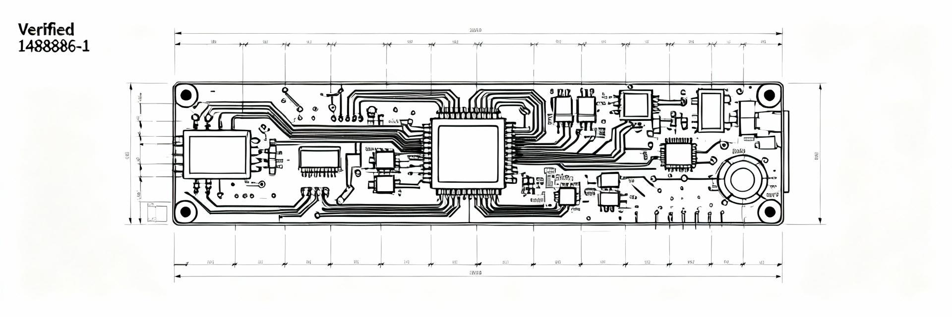
1488886-1 PCB Footprint Guide: Step-by-Step Build Tips
Mis-sized footprints are a frequent root cause of assembly failures, late re-spins, and unexpected costs. This guide addresses a concrete workflow to produce a verified 1488886-1 PCB footprint, minimizing solder defects, placement errors, and mechanical interference. Engineers who follow the steps below will be able to generate a CAD-accurate land pattern and hand off production-ready files with clear inspection points.
This footprint guide lays out a repeatable process: extract datasheet parameters, map pins to pads, calculate mechanical envelopes, set pad and mask rules, run focused DRC, and prepare a production handoff checklist. Each section includes prescriptive defaults, tolerance formulas, and verification steps so you can deliver a footprint ready for fab and assembly review.
(1) Why a Correct 1488886-1 PCB Footprint Matters — Background & Risk Profile
(1.1) Datasheet essentials to capture
Start by recording pin pitch, pad geometry, recommended land pattern, leadframe/mechanical outline, and all tolerances from the datasheet into a single reference table. Capture units (mm), tolerance class, and reference datums. This single-source table reduces transcription errors and gives CAD input a verifiable origin for pad dimensions and placement coordinates.
(1.2) Common failure modes and real costs
Solder bridging, tombstoning, component skew, and mechanical interference are typical failures tied to footprint errors. Quantify impact: rework per board can be hours of labor and scrap can cascade into shipment delays. Tag critical failures by likely root cause to prioritize DRC rules and first-article inspection for high-risk footprints.
(2) Pin Mapping & Mechanical Constraints — Data-Driven Checks
(2.1) Building a pin-to-pad mapping table
Create a simple CAD-ready table listing pin number, net name, nominal X/Y coordinate relative to package datum, and pad ID. For asymmetric or rotated packages include a rotated-coordinate column and a visual key. This mapping prevents pin-swap errors during footprint creation and supports automated pick-and-place exports.
(2.2) Clearance, tolerance, and mechanical envelope calculations
Use manufacturing tolerances to calculate solder mask clearance, courtyard margins, and keepout envelopes. Formula examples: pad expansion = pad_nominal + fab_tol; courtyard = max(package_outline + 0.5 mm, pad_extents + assembly_margin). This footprint guide uses these rules to set safe defaults while allowing tight-pitch adaptation where necessary.
(3) Step-by-Step Footprint Build Workflow — From Datasheet to Pads (Methods)
(3.1) Setting pad sizes, shapes, and plating considerations
Select pad shape by leadframe termination: rectangular pads for gull-wing or flat terminations, rounded for fillet-prone surfaces. Rule of thumb: pad length ≈ 1.0×lead length to allow adequate fillet; pad width based on recommended land pattern plus manufacturing tolerance. Consider via-in-pad only if assembly vendor supports filling and cap plating.
(3.2) Silkscreen, courtyard, and solder mask definitions
Place reference designators outside the courtyard and set silkscreen offset ≥0.2 mm from pad edges. Set solder mask expansion to −0.05 mm for fine-pitch pads or 0.05 mm for standard processes. Define courtyard as package outline plus 0.5 mm minimum to ensure tooling clearance and fiducial visibility for assembly alignment.
(4) Verification & DRC: Checks to Avoid Costly Re-spins (Methods/Quality)
(4.1) A practical DRC checklist for 1488886-1 PCB footprint
Automate spacing, annular ring, pad-to-pad minimums, and mask clearance checks in your CAD DRC. Manually verify pick-and-place center alignment, silkscreen truncation, and mechanical keepouts. Flag any DRC overrides with documented justification and reviewer initials to avoid silent fixes that cause late-stage surprises.
(4.2) 3D mechanical fit, stencil, and thermal verification
Load the component 3D model into the board assembly and check height, keepout interactions, and enclosure clearance. For the stencil, follow paste aperture-to-pad area ratios (typically 60–90% paste-to-pad for small pads) and split apertures for thermal reliefs. Verify paste coverage with a CAD paste view before export.
(5) Walkthrough Case Study — Building the Footprint (Practical Example)
(5.1) Step-by-step annotated example (screenshots/steps)
Sequence: extract dimensions → map pins → create pad geometry → apply mask rules → define courtyard → run DRC → generate fabrication outputs. Capture each step as an annotated image showing datum alignment, pad-size decisions, and final DRC pass. These annotations become the review artifact for mechanical and assembly teams.
(5.2) Troubleshooting log: common mistakes and fixes
Typical fixes: increase pad length for poor fillet, reduce mask expansion for bridging, correct pad rotation for asymmetric packages. Maintain a short troubleshooting log entry per issue: symptom, root cause, corrective action, and verification test (visual + DRC). This log speeds future reviews and reduces repeated errors.
(6) Production Handoff & Final Checklist — Ready for Fab & Assembly (Actionable)
(6.1) Files and notes to include for manufacturers
Bundle Gerber/ODB++ with clearly labeled paste/stencil files, 3D model, and a single-page commissioning note listing critical tolerances, inspection points, and any special assembly instructions such as nonstandard paste apertures or polarity markers. Include pick-and-place CSV with reference designators and rotation data.
(6.2) Final QC steps and sign-off criteria
Establish cross-team sign-off: layout, mechanical, and assembly leads must confirm footprint critical dimensions and DRC clearance. Tag high-risk footprints for first-article inspection and include a test coupon where practical. Record sign-off with date and reviewer ID to create an auditable handoff trail.
Summary (10–15% of total; ~150–225 words)
Follow a documented, data-driven process: extract datasheet parameters, map pins, set pad and mask rules, run targeted DRC, and prepare a concise production handoff. Applying these steps reduces solder defects, placement problems, and costly re-spins. A verified 1488886-1 PCB footprint is the result of disciplined verification and cross-team sign-off before fabrication.
- Capture mandatory datasheet parameters (pin pitch, pad dims, tolerances) into a single table to avoid transcription errors and provide CAD input traceability.
- Use formulaic clearance and courtyard calculations to set robust solder mask and assembly margins while adapting defaults for tight pitches.
- Run automated DRC plus manual 3D and stencil checks; bundle Gerber, paste, 3D models, and clear commissioning notes for manufacturer handoff.
FAQ
How do I verify the 1488886-1 pad dimensions quickly?
Cross-check pad dimensions extracted into your CAD against the datasheet table using a scripted or spreadsheet-based comparison. Verify X/Y coordinates relative to the package datum and run a targeted DRC for pad width, length, and spacing. A quick 3D overlay validates mechanical fit and reveals obvious misalignments before exporting fab files.
What paste aperture rules apply for this footprint?
Start with a paste-to-pad area ratio around 60–80% for small SMD pads; reduce if tombstoning is observed. For long rectangular pads consider a split aperture pattern to control paste volume. Confirm stencil thickness and aperture shape with your stencil vendor and validate paste coverage using the CAD paste view prior to production.
Which files should accompany the footprint to avoid assembly delays?
Provide Gerber or ODB++ plus dedicated paste/stencil files, the component 3D model, pick-and-place CSV, and a short commissioning note highlighting critical dimensions, tolerances, and inspection points. Clear documentation of any deviations from recommended land patterns speeds up manufacturer questions and reduces hold-ups in production.