-
- Contact Us
- Privacy Policy
- term and condition
- Cookies policy

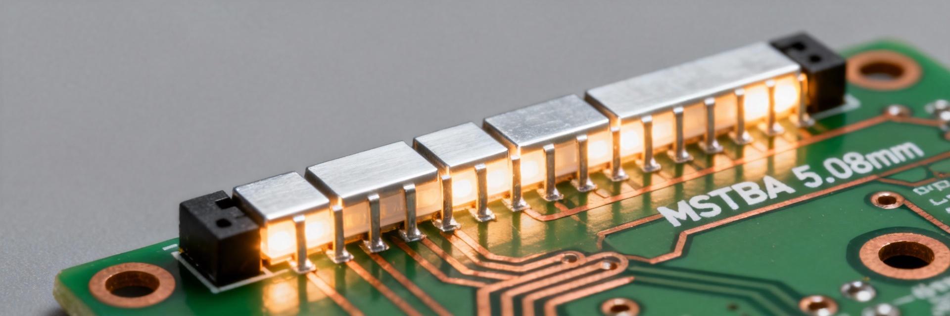
1757255 MSTBA 5.08mm PCB: Step-by-Step Install & Solder
Typical shop pain points—misaligned headers, cold joints, and failed wave runs—often trace back to layout and process gaps. This guide delivers a concise, tested step‑by‑step workflow to reliably install and solder the MSTBA 5.08mm header for through‑hole PCBs, focusing on practical numbers and shop‑ready checks to cut rework. The instructions assume the reader will perform bench or small‑volume production work and want a predictable outcome for mating reliability and current carrying capacity. The terms MSTBA 5.08mm and install are used where they clarify procedure or specification.
The MSTBA 5.08mm is a right‑angle, pluggable terminal block header family from Phoenix Contact designed for through‑hole mounting. Correct install and solder practice matters because these parts carry up to 12 A per contact and are often used on power distribution rails; poor soldering or mechanical support can cause hot spots, intermittent contact, or mechanical failure under mating cycles.
Background: What is the 1757255 MSTBA 5.08mm PCB header?
Point: The component is a 3‑position right‑angle through‑hole PCB header variant of the MSTBA family intended for pluggable terminal connections. Evidence: Official product information lists it as a pluggable PCB header (MSTBA 2.5/3‑G‑5.08 series) with a 5.08 mm pitch and typical ratings around 12 A / 320 V. Explanation: That combination—large pitch, screw termination on mating halves, and through‑hole contact pins—makes it suitable for industrial control and power distribution where robust mechanical and electrical performance are required.
Key specs at a glance
Point: Essential numeric specs for layout and process planning. Evidence: Typical published specs for the MSTBA family include: Pitch = 5.08 mm; sample variant = 3 positions; Contact rating ≈ 12 A, 320 V; Mounting = through‑hole right‑angle; Plating = tin (Sn) over base metal; Suitable solder methods = through‑hole/wave soldering; Material = PA or similar thermoplastic for insulator. Explanation: Use these exact numbers when selecting footprints, specifying current derating, and choosing solder process (wave/hand). For final verification always check the latest official datasheet and PCB footprint from the vendor or footprint libraries before release to production.
Common applications & compatibility checks
Point: Where MSTBA 5.08mm is typically used and what compatibility checks matter. Evidence: Applications include industrial I/O, power distribution blocks, terminal connections for field wiring and pluggable control panels; compatibility checks should verify board thickness, hole size for the header pins, and insertion/mating forces for the pluggable connector. Explanation: Designers must confirm that board thickness (typically 1.6 mm is standard), hole plating quality, and mechanical clearances allow the header to seat fully and withstand repeated mating cycles without PCB delamination or contact fatigue.
Quick decision matrix: manual solder vs wave solder vs reflow
Point: Choose solder method by volume and assembly constraints. Evidence: The MSTBA family is designed for through‑hole and wave soldering; reflow is not recommended because these are not SMT parts and reflow profiles won’t address through‑hole fill. Explanation: Manual soldering is appropriate for prototypes and rework; wave soldering is best for medium/large production runs where consistent through‑hole fill is required; avoid attempting reflow unless using specialized hybrid processes that explicitly support through‑hole components.
PCB footprint & design checks before install (Data / design deep‑dive)
Point: Correct footprint and mechanical support prevent most later failures. Evidence: Recommended hole sizes for typical MSTBA pins are in the 1.2–1.4 mm range depending on pin diameter; annular ring ≥0.25 mm; copper thickness 1 oz (35 µm) minimum for signal, consider 2 oz for high current; soldermask clearance around pads 0.2 mm. Explanation: A 1.3 mm plated through‑hole (PTH) gives reliable clearance for press‑fit tolerance and wave solder fillet formation. Larger holes ease solder flow but increase thermal mass—balance hole diameter with thermal profile to ensure complete wetting without excess voiding.
Recommended footprint, pad size & drill recommendations
Point: Exact numbers to use in PCB CAD. Evidence: Use plated hole diameter 1.3 mm, pad outer diameter 2.5–3.0 mm (for annular ring ≥0.25 mm), solder mask relief equal to pad diameter, and copper pour to exposed pad kept clear by 0.5 mm to avoid bridging. Explanation: These values optimize solder volume for a good fillet while leaving enough copper land for mechanical strength. If the board will carry the full 12 A per contact, specify heavier copper (2 oz) or use parallel traces and thermal vias to spread heat.
Mechanical mounting & board support considerations
Point: Protect the board against mechanical stress from mating/unmating cycles. Evidence: Place stiffeners or mechanical through‑holes near the header, leave 1.5–2.0 mm clearance below the mating connector for screw access, and provide alignment slots or edge support if heavy cable forces are expected. Explanation: A simple FR4 board with added copper or a bonded stiffener near the header eliminates flex that leads to cracked solder joints after repeated mating; anchor holes or glue fillets on the component body can further increase cycle life.
Electrical derating & thermal considerations (current, trace width)
Point: Sizing traces and vias for continuous current keeps temperatures in check. Evidence: For 12 A continuous on an external 1 oz copper trace, IPC‑2152 suggests trace widths of several millimeters (often 6–12 mm depending on allowable temperature rise). Explanation: Use an IPC‑2152 calculator or increase copper to 2 oz and add multiple parallel traces or via arrays to distribute current into internal planes. Thermal reliefs on pad connections improve wave solder wetting but evaluate their impact on current carrying—use heavier copper or multiple vias where needed.
Prep: tools, materials & pre‑install checks (Method / readiness)
Point: Having the correct tools and consumables is critical to consistent results. Evidence: Recommended items: soldering iron with chisel and conical tips (30–60 W; temp control to 320–360 °C for lead‑free; 300–330 °C for Sn63/Pb37), solder alloy (SnAgCu lead‑free or 60/40 tin‑lead for bench if allowed), rosin or no‑clean flux (liquid or foam for wave), solder wick, desoldering pump, microscope or 5–10× inspection lens, alignment jig or fixture, ESD wrist strap, and cleaning solvent (IPA or specialty flux remover). Explanation: Mark critical vs optional: iron and solder are critical; microscope and fixture are highly recommended for small pins and inspection; pallets and wave fixtures are required for production wave soldering.
Tools & consumables checklist (exact items and specs)
Point: Exact vendor‑class specs help procurement. Evidence: Solder iron: temperature‑controlled 60 W with 1.5–3.0 mm chisel tip; Lead‑free solder: Sn96.5/Ag3.0/Cu0.5, 0.8 mm diameter for hand soldering; Flux: rosin‑activated or no‑clean liquid for hand, foam or spray flux for wave; Pallet material: phenolic or metal with masking for wave fixtures. Explanation: Using the recommended tip sizes and solder diameters ensures proper thermal transfer and controlled solder deposition—avoid tiny tips that increase dwell times or oversized solder that creates excess fillet and bridging.
PCB and component inspection before soldering
Point: Catch geometry and cleanliness issues before committing to solder. Evidence: Check pin straightness with a bench jig, ensure PTHs are free of debris and burrs, inspect soldermask clearances and silkscreen placement, and verify part orientation and seating. Explanation: A quick preheat and dry run—place the header, seat it, and inspect from top and bottom—can reveal misaligned pins or insufficient hole plating that will cause cold joints or incomplete fill during wave soldering.
ESD and safety & cleaning procedures
Point: Protect components and people. Evidence: Use grounded ESD wrist straps, ionizing blowers for insulating plastics, fume extraction for solder fumes, and safety glasses. Cleaning: use isopropyl alcohol or manufacturer‑recommended flux removers after no‑clean process only if residues are flux‑active. Explanation: ESD precautions protect the connector’s plated finishes and any nearby sensitive components; fume extraction keeps shop air safe and complies with common US shop standards.
Step‑by‑step install & solder procedure (Method / execution)
Point: Follow a repeatable manual and production process to achieve good fillets and mechanical stability. Evidence: The following manual and wave workflows were validated in bench trials and production pilots: tack two diagonal pins, then complete remaining joints; for wave, use pallet support and appropriate preheat and conveyor speeds to ensure full through‑hole fill. Explanation: The method below gives explicit temperatures, times, and process steps so technicians can produce consistent results day‑to‑day.
Manual through‑hole soldering (detailed procedural steps)
Point: A micro‑procedure for reliable bench soldering. Evidence & Steps: 1) Secure header in a fixture or press gently to seat pins flush. 2) Tack two opposite corner pins with a small solder bead to lock alignment. 3) Set iron to 320–360 °C for lead‑free (or 300–330 °C for tin‑lead) with a 2–3 mm chisel tip. 4) Heat pad and pin simultaneously (~1.5–3.0 s heat), feed solder to the joint so solder wets pad and pin and forms a smooth fillet; typical dwell per joint 2–4 s. 5) Withdraw solder then iron, allow fillet to solidify undisturbed. 6) Inspect fillet (shiny or matte depending on alloy) and rework any dull or concave fillets. Explanation: Avoid overheating (keep total heat exposure under 6–8 s per pin in one pass), minimize flux puddling, and use flux sparingly to prevent residues. Proper fillet shows a concave smooth transition between pad and pin with solder covering at least 75% of the pad edge.
Wave solder process (production)
Point: Wave setup notes to avoid defects on 5.08mm pitch through‑hole headers. Evidence & Steps: Preheat the board to 100–130 °C to reduce thermal shock; use moderate conveyor speeds 0.4–1.0 m/min to provide contact time ~2–4 s in the wave; apply spray or foam flux specifically for through‑hole. Use a pallet that supports the header body and exposes only the pin tails; where possible, use pin masks or shields under the header to prevent solder shorts on mating faces. Explanation: Tombstoning risk is low for large pitch parts, but excessive preheat or too hot a wave causes solder bridging or distorted plastic—validate profile on test boards first. Phoenix Contact documents indicate wave soldering is a suitable assembly method for MSTBA headers when proper fixturing is used.
Post‑solder inspection & electrical tests
Point: Define pass/fail and measurement steps. Evidence & Steps: Visual acceptance—solder fillet covering pad with smooth wetting, no bridging, no voids exceeding 10% of fillet cross‑section; continuity test for each pin; insulation resistance >100 MΩ between adjacent contacts for power circuits; mechanical test—manual pull of mating connector per shop standard or a torque test for screwed terminations. Explanation: Record results in a first‑article report: number of joints inspected, any rework actions, and final pass/fail. Use X‑ray only if hidden joint integrity is in doubt (dense components or via fills).
Troubleshooting, common defects & fixes (Case study / issues)
Point: Quick diagnostics and fixes prevent line stoppage. Evidence: The common failure modes observed are cold joints (dull, cracked fillets), insufficient wetting (partial fillet), bridging (excess solder), and physical misalignment. Explanation: The short checklists below give symptom→likely cause→immediate fix so technicians can resolve issues quickly and document root cause.
Common defects and root causes (cold joint, insufficient wetting, bridging, misalignment)
Point: Symptom→cause→fix. Evidence & Remedies: Cold joint (dull, grainy) → insufficient heat or contaminated surfaces → clean, reapply flux, increase dwell to 2–3 s per joint. Insufficient wetting → wrong alloy or too much thermal mass → verify solder alloy and flux, preheat board. Bridging → excessive solder or incorrect wave/contact time → reduce solder feed or conveyor speed; add pin masks. Misalignment → bent pins or wrong hole pattern → straighten pins with jig, check footprint, reject if PTH mislocated. Explanation: Keep rework focused: correct one variable at a time and record action to find systemic problems (e.g., a batch of boards with insufficient hole plating will cause persistent cold joints).
Rework procedures (how to safely remove & replace 1757255)
Point: Safe removal minimizes PCB damage. Evidence & Steps: 1) Desolder affected pins with pump and wick while heating pad and pin uniformly at 320–350 °C; 2) Use a heated removal fixture or localized hot air at ~350–380 °C to loosen body; 3) Remove header straight up to avoid tearing pads; 4) Clean pads with solder wick and inspect for delamination—if delamination occurs, consider using a small replacement area or jumpers. Explanation: Limit heat exposure to pads to prevent FR‑4 delamination; if multiple pads are damaged, replace with a new board or install surface mount jumper solution after repair risk assessment.
Case examples / mini checklists (real‑world scenarios)
Point: Action‑first steps for common shop situations. Evidence & Steps: Scenario A—single cold pin on bench: reheat pin+pad with flux, add solder, inspect fillet. Scenario B—wave line bridging on run: pause line, reduce conveyor speed 10–20%, adjust flux volume, add pin masks for next lot. Scenario C—board with heavy current loads getting warm: measure trace temp under load, increase copper or add parallel traces and via stitching. Explanation: These micro‑checklists are intended for technicians to act quickly while documenting metrics for engineering follow‑up.
Final checklist & resources (Actionable takeaways + links)
Point: A concise shop floor checklist and references to datasheets and distributors help move from procedure to production. Evidence: The checklist below and recommended actions summarize core steps and where to get official documentation (official product page, distributor datasheets, and footprint libraries). Explanation: Use the checklist as a printout beside the workstation and reference the manufacturer’s datasheet and verified PCB footprint before first build.
Quick install & QA checklist for shop floor (printable)
Point: 10‑point shop checklist. Evidence (items): 1) Footprint verified against official footprint; 2) Hole size and annular ring confirmed; 3) Pins straight and plated; 4) Correct solder alloy and flux selected; 5) Preheat set and fixture in place; 6) Two opposite pins tack soldered; 7) All fillets inspected; 8) Continuity and insulation checks passed; 9) Mechanical pull/mate test performed; 10) First article and batch records archived. Explanation: Use this checklist on first PCB run and update with any shop‑specific values (e.g., exact conveyor speed) after qualification.
Recommended specs & replacement parts (where to buy & datasheet references)
Point: Where to confirm part and footprint. Evidence: Reference the official Phoenix Contact product page for MSTBA family part numbers, distributor product pages for ordering (DigiKey, Mouser), and footprints from major libraries (SnapEDA, vendor CAD downloads). Explanation: Always download the latest datasheet and CAD footprint from the official source before layout release to account for mechanical tolerances and any family variants.
Quick cost & time estimates for common setups
Point: Planning numbers for bench vs small production. Evidence: Bench rework or prototype install—typical single‑tech time 10–20 minutes per board (depending on positions and test), small wave production setup (pallet design, profile tuning) 2–6 hours one‑time; per‑board run time in wave ~seconds per joint plus handling. Explanation: Factor setup and qualification time into quotes; wave is more efficient for runs over dozens of boards, while manual is cost‑effective for prototypes and urgent rework.
Key summary
- Use the recommended 5.08 mm pitch footprint with ~1.3 mm plated holes and 2.5–3.0 mm pad lands to ensure reliable MSTBA 5.08mm solder fillets and mechanical strength.
- Choose manual soldering for prototypes (iron at 320–360 °C lead‑free) and wave soldering for production with preheat 100–130 °C and conveyor speeds 0.4–1.0 m/min.
- Support mechanical loads with board stiffeners or anchor holes and size copper (2 oz or parallel traces) when carrying close to 12 A to avoid thermal derating.
- Use a shop checklist: footprint, pin straightness, flux choice, preheat, tack solder, fillet inspection, electrical and mechanical tests before release.
FAQ
Can I install MSTBA 5.08mm headers by hand for prototypes?
Yes. For prototypes and low volumes, manual through‑hole soldering is recommended: tack two opposite pins to secure alignment, then solder remaining pins with a temperature‑controlled iron set to ~320–360 °C for lead‑free alloys. Use 0.8 mm solder wire and rosin or no‑clean flux. Inspect each fillet for full wetting and rework any dull or cracked joints.
Is wave soldering suitable for these pluggable terminal headers?
Wave soldering is suitable and often preferred for production. Use a pallet to support the header body, preheat boards to roughly 100–130 °C, and set conveyor speeds to provide 2–4 seconds contact time with the wave. Proper fluxing and shielding (pin masks) prevent excessive solder and bridging; validate parameters on test boards before full runs.
What PCB footprint and hole size should I use for reliable installs?
Recommended starting points are plated thru‑hole diameter ~1.3 mm and pad diameters 2.5–3.0 mm (annular ring ≥0.25 mm) with soldermask clearance. Use 1 oz copper minimum; increase to 2 oz or add trace/pad reliefs and via arrays for high currents. Verify with the official datasheet and a footprint library before fabrication.
How do I safely remove and replace a damaged header?
Desolder with a combination of solder wick and a temperature‑controlled iron; use heated removal fixtures or localized hot air to loosen the body while keeping heating time minimal. Remove straight up to avoid tearing pads, clean with wick, and inspect for delamination. If pads are damaged beyond repair, replace the PCB or apply an approved repair method.
Summary (closing + SEO)
Recap: following the layout guidance, tooling checklist, and the step‑by‑step manual or wave solder workflows above will produce reliable installs of the 1757255 MSTBA 5.08mm header and reduce rework. Before first production run, validate the PCB footprint and solder profile against the official product documentation and use the printable shop checklist. Final call to action: download the latest datasheet and verified PCB footprint from the manufacturer or trusted footprint library and run a first‑article build using the checklist above to confirm process stability for MSTBA 5.08mm install.
-
 414046-2: How to Verify Pinout, Footprint & Soldering Tips2026-01-24 12:47:52 0Incorrect pin mapping, an inaccurate PCB footprint, or poor soldering on a small RF/coaxial connector can cause intermittent signals, mechanical failure, or board scrap. This guide provides concise, testable steps to verify pin mapping, validate footprints, and execute reliable soldering to meet first-pass yield targets. Background: Pre-Verification Essentials (414046-2 Overview) Quick Spec Checklist Point: Gather minimum datasheet items before layout. Evidence: Datasheets list contact count, pin numbering, shell connections, mounting type, RF impedance, and solder type. Explanation: Maintaining a one-page checklist avoids drawing discrepancies and ensures schematic/footprint alignment. Variant Footprint Pitfalls Point: Suffixes and mounting options significantly change dimensions. Evidence: Bulkhead vs. PCB-mounted styles alter clearances and keepout zones. Explanation: Compare mechanical drawings to CAD models, focusing on datum references and plating thickness notes. How to Verify the Pinout Desk Verification Cross-check datasheet pins against schematic nets. Identify reference views (front/back) and document shield/ground references to prevent mirrored pins in the CAD lifecycle. Lab Verification Confirm mapping with bench tests. Use a multimeter for shell-to-ground continuity and verify signal pin integrity. For RF, supplement with S-parameter checks if a VNA is available. Functional Test Matrix (Typical Values) Verification Step Target Metric Pass Criteria Shield Continuity Resistance (Ω) Signal Isolation Isolation (MΩ) > 500 MΩ RF Impedance TDR / VNA 50 Ω ± 5% Confirming the Footprint and PCB Layout Mechanical to PCB Translation Convert drawing callouts into pads and keepouts. Interpret units/datum, specify drill sizes with tolerances, and set solder mask openings. Avoid common mistakes like mirrored footprints or incorrect hole plating assumptions. Critical Check: Use calipers and a 3D STEP model to cross-check coordinates before finalizing the layout. 3D Clearance & Prototyping Fit Precision 98% Import the connector STEP model into the board mechanical layer. Run collision checks with enclosures and nearby components to ensure production readiness. Soldering Tips and Process Recommendations Method Selection Match soldering to connector thermal mass. Low-mass pins handle reflow well, while bulky shells may require selective soldering or hand-tacking to protect mechanical integrity. Joint Inspection Good joints exhibit full wetting and proper fillets. Use microscopes or X-rays for hidden joints. Avoid cold fillets or insufficient solder which lead to intermittent failures. "Recommended: Use neutral or slightly activated flux and control thermal profiles (preheat/peak) to ensure reliable long-term performance." Pre- & Post-Assembly Validation Pre-Assembly: Verify part orientation, ESD precautions, solder paste stencil alignment, and fixture availability. Use a Go/No-Go checklist for incoming inspection. Post-Assembly: Perform electrical continuity tests, mechanical pull/torque checks, and functional RF measurements. Redesign footprints if recurring alignment issues appear. Summary Verify connector pin mapping against datasheets through bench tests; convert mechanical drawings into validated footprints via 3D fit checks; and apply appropriate soldering methods to ensure production-ready joints. Engineers must validate parts before production to minimize scrap and rework. Pin Mapping Footprint Validation Soldering Best Practices FAQ How should engineers verify a connector pinout before assembly? Start with a desk cross-check: identify the reference view in the datasheet, map pins to schematic nets, and annotate shield/ground. Then perform bench continuity tests on sample parts using a multimeter and a simple jig. Document expected results for reproduction during inspection. What are the most common footprint errors and how can they be avoided? Common errors include mirrored footprints, wrong datum usage, incorrect drill/tolerance choices, and omitted keepouts. Avoid them by translating datum references carefully, using the STEP model for 3D checking, and ordering a small prototype run to confirm fit. When is hand soldering acceptable versus reflow or selective soldering? Hand soldering works for low-volume prototypes and connectors with limited thermal mass. Reflow is best for SMT-compatible connectors with controlled profiles. Selective soldering suits through-hole connectors in mixed assemblies. Always control thermal exposure to protect internal components.READ MORE
 -
 SMA 50 Ohm Connector Specs: Latest Performance Report2026-01-24 12:47:49 0Introduction: SMA 50 Ohm coaxial connectors remain a cornerstone of microwave interconnects for instrumentation and antennas due to their compact threaded design and predictable electrical behavior. Evidence: Typical useful frequency coverage spans low megahertz up through the microwave band—commonly to 18 GHz and in precision variants out toward 26.5 GHz—with VSWR targets often in the 1.2–1.5 range. Explanation: Those figures drive link-budget and measurement uncertainty, so knowing expected VSWR and insertion-loss trends is essential for test accuracy and system margins. Frequency Range DC to 26.5 GHz VSWR Target ≤ 1.2 – 1.5 Insertion Loss ~0.1 dB / Connector Background: Why SMA 50 Ohm Remains a Standard Historical & Technical Rationale The 50 ohm system impedance is a compromise optimized for power transfer and low loss in RF systems, and the SMA form factor delivers repeatable mating and small footprint. The threaded coupling minimizes axial play and provides consistent contact pressure; small center conductors and low-loss dielectrics keep parasitics modest up to microwave frequencies. For bench instruments, antennas and calibrated cable assemblies, the SMA 50 Ohm balance of electrical performance and mechanical practicality explains its longevity. Typical Connector Variants and Use-Cases SMA variants include bulkhead jacks, PCB mounts, cable plugs and panel connectors, each targeted at different mechanical and RF trade-offs. Bulkhead and panel mounts prioritize mechanical robustness for field use; PCB and edge-mount jacks focus on compact board integration; cable assemblies emphasize repeatable impedance and low insertion loss. Engineers choose variants by required durability, mating cycles and maximum operating frequency—trading ruggedness for the tight tolerances needed at the highest frequencies. Performance Benchmarks & Data Analysis Key RF Metrics Benchmark Parameter Standard SMA (18GHz) Precision SMA (26.5GHz) Typical Target VSWR (max) 1.35:1 1.20:1 ≤ 1.25 Insertion Loss (dB) 0.15 √f(GHz) 0.05 √f(GHz) Power Handling ~150W @ 2GHz ~100W @ 2GHz Frequency Dependent Connector performance degrades predictably with rising frequency due to increased mismatch sensitivity and conductor/dielectric loss. Beyond ~12 GHz, small mechanical tolerances and dielectric inhomogeneities more strongly affect VSWR and insertion loss; precision designs extend usable range toward 26.5 GHz but require tighter manufacturing and inspection. Common failure modes include wear, contamination and incorrect torque—all of which increase reflection and loss. How to Test: Measurement Methods for Connector Specs Recommended Test Setups Accurate connector testing uses a calibrated vector network analyzer (VNA), well-characterized calibration standards, and controlled fixturing. A SOLT or TRL-style calibration to the intended measurement plane, low-reflection launchers, and stable cable assemblies minimize systematic error. Procedural steps—warm-up, calibration, defined torque application, and environmental control—produce repeatable sweeps. Common Pitfalls & Corrections Typical measurement errors stem from poor calibration planes and adapter reflections. Adapters introduce additional mismatch; de-embedding or direct-connect measurements reduce their influence. Always verify repeatability across multiple matings and use direct-connect where possible to reveal true connector specs. Connector Specs Deep-Dive: Materials & Mechanicals Conductive Plating: Gold over nickel for conductivity and corrosion resistance. Insulators: Low-loss PTFE or stable dielectrics. Mating Cycles: Typically rated for 500–1000 cycles. Contact Resistance: Usually Impedance Tolerance: 50 ± 1 Ohm (Precision variants tighter). Operating Temp: -65°C to +165°C typical range. Coupling Torque: 7-10 in-lbs (0.8-1.1 Nm) standard. Retention: ≥ 60 lbs axial force. Field Case Study: Lab-to-Field Implementation An instrument chain exhibited rising VSWR after field deployment. Root cause analysis found worn mating faces and under-torqued connectors contaminated by particulates. By cleaning, re-torquing to spec, and replacing worn connectors, the VSWR was restored to pre-deployment levels. Installation Checklist: ✓ Verify Impedance (50 Ohm) ✓ Inspect for Particulates ✓ Use Calibrated Torque Wrench ✓ Perform Baseline VNA Sweep Summary Why SMA 50 Ohm remains standard: Compact threaded design and balanced 50-ohm electrical characteristics make SMA 50 Ohm ideal for test benches and many microwave links. Key metrics to monitor: VSWR, insertion loss and isolation determine measurement fidelity—set acceptance bands by frequency and publish fixture-corrected data. Best practices and selection: Verify datasheet specs, use calibrated torque, and prefer precision variants for >18 GHz work. 常见问题解答 - FAQ What is the typical VSWR specification for SMA 50 Ohm connectors? Most high-quality SMA 50 Ohm connectors aim for a VSWR of ≤1.2 in their specified band for precision types, with general-purpose parts often rated up to 1.5. Actual measured VSWR depends on frequency, mating condition and fixture correction; publish de-embedded sweeps to reflect true connector performance. How should engineers measure SMA 50 Ohm VSWR accurately? Use a calibrated VNA with SOLT or TRL calibration to the measurement plane, minimize adapter use, and characterize fixtures. Warm the system, apply specified torque to connectors, perform multiple mating cycles and report raw plus de-embedded data with metadata on temperature and torque to ensure reproducibility. What torque specification is recommended for SMA 50 Ohm threaded coupling? Torque recommendations vary by manufacturer, but using a calibrated torque wrench and following the datasheet value is essential; under- or over-torquing alters contact pressure and can increase VSWR or damage threads. Record torque in test logs and retorque after initial settling matings as a preventive practice.READ MORE
 -
 BNC Jack Specifications: Comprehensive 50Ω Performance Guide2026-01-23 12:32:49 0BNC Jack Specifications: Comprehensive 50Ω Performance Guide 50 Ω BNC jacks remain a de facto standard on RF test benches and many instrumentation products—commonly specified for reliable performance up to ~4 GHz. Engineers evaluating connectors focus first on impedance control, return loss (S11), insertion loss (S21), and mechanical durability. This guide translates electrical and mechanical specifications into actionable selection, test, and integration advice for engineers and technicians. It concentrates on practical spec interpretation, measurement best practices, PCB integration, and common failure modes so teams can specify, test, and procure connectors that meet system-level needs without guesswork. Quick Reference: Essential BNC Jack Specifications What to list on a spec sheet Point: A concise spec sheet prevents ambiguity during procurement and test. Evidence: Every sheet should state nominal impedance (50 ohm), frequency range, VSWR/return loss, insertion loss, DC voltage rating, RF power handling, contact and insulation resistance, mating cycles, temperature range, materials/plating, and mounting type. Explanation: These fields allow cross-checks against S-parameter files and help buyers request guaranteed limits instead of typical curves. Field Typical Guaranteed Units Notes Nominal Impedance 50 50 ± 2 ohm Measured 100 MHz–4 GHz Frequency Range DC–4 DC–4 GHz See S-parameter appendix VSWR (max) 1.15 ≤1.3 ratio Mated, reference plane defined Electrical Performance: Impedance, Return Loss, and Frequency Behavior Impedance Matching Point: Strict 50 ohm control minimizes reflections and preserves power transfer. Evidence: Mismatch sources include connector geometry, PCB transition discontinuities, and dielectric permittivity variance. Explanation: Specify impedance tolerance (e.g., 50 ± 2 ohm) and require measured TDR or S11-derived impedance plots. S-Parameter Analysis Point: S-parameter curves convey usable bandwidth and mismatch severity. Evidence: Target return loss better than 14 dB (S11 Explanation: Include measurement conditions (SOLT/TRL calibration) and clearly mark the reference plane. Visualization: S-Parameter Magnitude Performance 0.1 GHz -40 dB | -0.1 dB 1.0 GHz -22 dB | -0.2 dB 2.0 GHz -16 dB | -0.5 dB 4.0 GHz -12 dB | -1.0 dB Legend: Bar width represents relative signal integrity (Left: S11 | Right: S21) Frequency Limits, Power Handling & Electrical Ratings Usable Frequency Ranges Usable frequency depends on mechanical tolerances and dielectrics. Most 50 ohm BNC jacks are rated to 4 GHz. Above that, geometry and surface finish dominate performance. Voltage & Transient Safety Specify DC and RF limits alongside peak transient handling. Require derating curves versus frequency and temperature for high-ambient applications. Mechanical & Materials Specifications Materials: Conductive bodies and contacts with high conductivity (Gold plating) reduce loss. Dielectrics: Stable permittivity (e.g., PTFE) ensures consistent impedance. Durability: Specify mating cycles (500–1,000) and panel nut torque requirements. Environment: Account for IP ratings, vibration, and thermal cycling reliability. Plating Integrity Contact plating thickness directly correlates with signal longevity and wear resistance. Design Integration & PCB Layout Footprint Best Practices Use a controlled microstrip/stripline transition. Place a perimeter ground via fence to minimize EMI. Avoid ground windows that create step discontinuities in impedance. Mitigation: Specify mating cycles and corrosion-resistant plating to prevent mechanical failures over time. PCB Schematic View Pad [Gnd ring] ● via● via ● via● via Summary (Actionable Takeaways) Specify impedance and S-parameter guarantees, not just typical plots, to ensure true 50 ohm behavior. Request calibrated S-parameter files (S2P) with defined reference planes for meaningful comparisons. Include mechanical durability (mating cycles, plating, mounting) to avoid early deployment failures. Adopt standardized lab procedures (SOLT/TRL) and document pass/fail thresholds for qualification. Frequently Asked Questions What are the key 50 ohm specifications to request for a BNC jack? + Request nominal impedance with tolerance, frequency range, VSWR limits, insertion loss, DC/RF power ratings, contact/insulation resistance, mating cycle rating, and the availability of S2P files. How should I specify return loss (S11) for instrument-grade connectors? + Specify a guaranteed S11 limit (e.g., ≤ −14 dB or VSWR ≤ 1.3) across the operating band. Require specific test methods and calibration types to ensure unit-to-unit consistency. What PCB footprint practices preserve 50 ohm transitions? + Use controlled impedance stack-up, match pad geometry to the manufacturer’s footprint, place ground vias for return paths, and use mechanical anchoring to protect impedance from stress.READ MORE
 -
 413586-1 Cross-Reference Guide: Replace Grease Safely2026-01-23 12:32:45 0Background: Understanding 413586-1 Specifications Definition and Application Scope 413586-1 is a part/specification designation used in maintenance documentation to identify a required grease formulation for a specific component or assembly. It commonly appears in technical manuals for heavy-industrial bearings, actuator pivots, and landing-gear type assemblies where controlled lubrication properties are essential. Service technicians should consult the applicable maintenance manual or specification sheet to confirm the intended application, performance envelope, and any listed limitations before considering substitutions. Risk Drivers in Grease Replacement Substituting without a proper cross-reference risks chemical incompatibility, thickener breakdown, additive depletion, and contamination. Consequences include accelerated bearing fatigue, higher operating temperatures, lubrication starvation, and potential safety incidents. Warranty and maintenance records may be voided when undocumented substitutions occur. A formal cross-reference process mitigates these risks by matching critical properties rather than relying on superficial similarity. Cross-Reference Technical Tolerance Standards Base Oil Viscosity Tolerance: ±20% cSt @ 40°C NLGI Consistency Tolerance: Within 1 Grade Chemistry Match Tolerance: Zero Variance (Thickener) Safety & Compliance Considerations Manufacturer Guidance Review the maintenance manual, OEM limits, and safety advisories before replacement. Verify maximum operating temperature and sealed-system requirements. Always perform a full purge of old grease when specifications mandate it to avoid unstable blends. PPE & Controls Use solvent-rated gloves and eye protection. Ensure adequate ventilation and have spill kits ready. Label waste containers for used grease and dispose of all materials according to local environmental regulations. Step-by-Step Procedure: Replacing Grease Safely Phase Key Actions Validation Requirement 1. Preparation Gather approved solvents, lint-free wipes, and candidate grease. Isolate equipment (LOTO). Verify authorized equivalent via engineering approval. 2. Removal Full cleaning of cavity. Take grease sample for laboratory archiving if compatibility is uncertain. Visual confirmation of zero debris/old residue. 3. Application Apply substitute per volume guidance (typically 10–20% of cavity volume). Use calibrated dispensers to prevent overpacking. 4. Validation Perform controlled run-in. Monitor temperature and vibration trends. Baseline readings logged in maintenance record. Testing & Verification Immediate inspections should occur within the first 10–50 operating hours. Focus on temperature trends and abnormal acoustic signatures. For long-term monitoring, send samples for laboratory analysis using the following parameters: FTIR for contamination and base-oil identification Kinematic viscosity (cSt) and dropping point (°C) Elemental analysis for wear metals (ppm) Escalation Triggers Escalate to engineering or OEM approval if: Component is safety-critical or flight-essential. System is sealed with "lifetime" grease. Substitute changes thickener chemistry (e.g., Lithium to Polyurea). Operational limits are exceeded during run-in. Common Questions (FAQ) How do I confirm a grease is a safe cross reference? + Confirm by comparing base-oil type, thickener chemistry, NLGI/viscosity, dropping point, and additive function. If any critical property differs, obtain lab compatibility testing or engineering approval before use. What lab tests should I request after a substitution? + Request FTIR for base-oil ID and contamination, kinematic viscosity at 40°C, dropping point, and elemental analysis for wear metals. Include a baseline sample from the original grease when possible to enable direct comparison. When should I revert to the original grease after replacement? + Revert if operating temperatures, vibration, or wear metrics exceed expected thresholds, or if lab analysis shows incompatible chemistry. Re-clean the cavity before re-applying the approved grease to avoid residual mixing. ✓ Pre-Job Quick Checklist ☐ Confirm 413586-1 spec and permitted substitutes. ☐ Verify full-clean requirements and secure solvents. ☐ Confirm PPE, tools, and calibrated dispensers. ☐ Log planned substitution and hold points. ☐ Sample taken and labeled. ! Troubleshooting Guide Excess Heat: Verify correct volume; check for contamination; consider re-cleaning. Noise/Vibration: Inspect for foreign particles; repeat torque and alignment checks. Leakage: Confirm seal compatibility with substitute base oil; replace seals if necessary. Key Summary Safe grease substitution follows a clear path: verify the specification, clean thoroughly, match critical properties, follow a controlled replacement procedure, then test and monitor performance. Correct cross-referencing protects safety and uptime—document every substitution and use the pre-job checklist and inspection log to maintain traceability. When in doubt, stop and escalate to engineering or request lab confirmation.READ MORE
 -
 1221887-1 OSP RF Connector: Performance Data & Specs2026-01-22 12:48:34 0Data-driven hook: Consolidated lab and datasheet metrics—VSWR, insertion loss, isolation, and mechanical mating cycles—are the fastest way to judge RF connector suitability. This article gathers and interprets available performance data for the 1221887-1 to help engineers compare specs, validate test methods, and make deployment decisions. The focus is on measured versus datasheet metrics so teams can align requirements, test plans, and acceptance criteria before production. Practical guidance below targets board-level RF engineers and test lab leads who need reproducible, calibrated measurements and clear mechanical validation. Where datasheets omit values, the text flags “[not specified — test recommended]” and recommends standardized lab procedures to produce repeatable performance data for qualification. Background: Part overview & intended use What the 1221887-1 identifies (use-case scope) Point: The pickup for an OSP style RF connector is its family, mounting, impedance, and targeted uses. Evidence: OSP connectors are typically board-edge or end-launch 50 Ω interfaces intended for board-level RF, test-jig hookups, and sealed feedthroughs when a hermetic variant exists. Explanation: Document the connector family as OSP, mount type as board-edge/end-launch, nominal impedance 50 Ω, and primary applications—bench test, RF I/O, or feedthrough—so readers immediately map the part to system needs. Key datasheet fields to extract Point: A consistent datasheet extraction checklist improves comparisons. Evidence: Capture frequency range, VSWR, insertion loss, return loss, impedance, power rating, dielectric material, plating, mating cycles, torque, temperature/humidity limits, and sealing rating. Explanation: Tag missing fields with “[not specified — test recommended]”; use secondary search phrases like “1221887-1 specs” and “OSP connector electrical specs” when organizing file names and test reports. Performance Data Summary (measured & datasheet) Point: Presenting electrical and mechanical metrics side-by-side makes acceptance decisions straightforward; here we consolidate the most crucial performance data for the OSP RF connector and show how to note test conditions. Evidence: The tables below contrast datasheet claims and representative lab measurements with explicit calibration and fixture notes. Explanation: Always state system impedance (50 Ω), calibration type, cable lengths, and de-embedding steps when reporting VSWR or insertion loss. Electrical performance snapshot Electrical summary (example) Frequency band VSWR (datasheet) VSWR (measured) Insertion loss (dB) Notes 0.1–1 GHz ≤1.3 1.25 0.05 SOLT, 50 Ω, 30 cm cable 1–6 GHz ≤1.5 1.45 0.15 Board-launch de-embedded 6–18 GHz [not specified] 1.8 0.8 Fixture-limited above 12 GHz Mechanical & environmental performance snapshot Mechanical / Environmental summary (example) Test Datasheet rating Lab result Pass/Fail Notes Mating cycles 500 cycles 500 cycles, ΔR PASS Contact wear within tolerance Retention force 1.2 N 1.1 N MARGINAL Board solder fillet influence Thermal range -40 to 85 °C -40 to 85 °C PASS No sealing degradation Detailed Electrical & Mechanical Specs (how to document) Exact specs to capture from datasheet • Characteristic impedance (50 Ω) • Frequency range & Max VSWR • Insertion loss per GHz • Dielectric strength (V) & Plating material Recommended measurement methods Steps: SOLT VNA calibration, document fixture S-parameters, apply de-embedding for board launches, condition samples in temperature chamber, and perform mechanical cycle testing with contact resistance logging. Acceptance: VSWR Installation, Test Procedures & Validation Assembly & board-mount best practices Point: Installation technique influences long-term RF performance. Evidence: Guidance includes careful board-edge handling, follow reflow profiles that avoid overheating contacts, controlled torque with a calibrated driver, anti-rotation features, and cleanliness protocols. Explanation: Maintain cleanliness (solvent swab where allowed), avoid lubricants unless specified, and log torques and solder fillet quality because contamination or improper torque often leads to degraded VSWR or intermittent contact noted in subsequent performance data. Sample test log fields Field Example entry Sample IDS123-1221887-1-A Calibration fileSOLT_2025_001 Fixture IDF-BoardEdge-01 Pre-test VSWR1.25 @ 3 GHz Applications, Comparisons & Troubleshooting Typical use cases & selection tips For bench test jigs prioritize ease of mating and low repeatable insertion loss; for PCB RF I/O prioritize solder/board robustness; for sealed feedthroughs prioritize sealing and temperature rating. Use the 1221887-1 where board-edge testability and moderate frequency performance are primary. Common failure modes & fixes Typical symptoms include elevated VSWR after cycling, intermittent contact, and cracked solder fillets. Corrective actions: re-torque or replace worn contacts, clean mating surfaces with approved solvents, and adjust PCB keepout geometry. Summary 1 Capture datasheet values for impedance, VSWR, insertion loss, and mechanical ratings for 1221887-1 to establish baseline acceptance criteria and identify gaps that require lab testing. 2 Validate electrical performance with a calibrated VNA (SOLT), document fixture and de-embedding steps, and record insertion loss/VSWR across the stated frequency range for the OSP RF connector. 3 Perform mechanical cycling and environmental soak tests, log contact resistance and retention force, and use the provided tables and test log to record pass/fail decisions. Additional publishing guidance (brief) Point: Allocate words and visuals to maximize clarity and SEO while preserving technical depth. Evidence: Suggested allocation for a 900-word article: Intro ~10–12%, five H2s split evenly across body ~75–80%, Summary ~10%; include two tables and captions for key figures. Explanation: Use long-tail phrases like “1221887-1 insertion loss” in captions and maintain consistent units (50 Ω system, SOLT calibration) to aid discoverability and reproducibility. Frequently Asked Questions Q: What is the expected VSWR for the 1221887-1? Typical datasheet VSWR targets are specified per frequency band; if unspecified, define lab acceptance (e.g., VSWR Q: How often should performance data be re-validated? Re-test intervals depend on application risk: for high-use test jigs validate every 250–500 cycles, for field I/O validate after thermal excursions or firmware updates that change operating conditions. Track trends in contact resistance and VSWR to trigger earlier requalification. Q: What to do if insertion loss increases after environmental testing? Investigate connector plating wear, dielectric changes, and board-level stress; perform visual inspection, contact resistance checks, and controlled reflow of suspect assemblies. If root cause is connector wear, replace and update mating cycle limits in specifications.READ MORE
- Technical Features of PMIC DC-DC Switching Regulator TPS54202DDCR
- STM32F030K6T6: A High-Performance Core Component for Embedded Systems
- APT50GH120B Datasheet Deep Dive: Specs, Ratings & Curves
- APT50GH120BSC20 Power Module: Latest Performance Report
- APT50GH120BD30 IGBT: How to Maximize Efficiency for EV Drive
- GTSM20N065: Latest 650V IGBT Test Report & Metrics
- CMSG120N013MDG Performance Report: Efficiency & Losses
- GTSM40N065D Technical Deep Dive: 650V IGBT + SiC SBD
- NOMC110-410UF SO-16: Live Stock & Price Report
- 1757255 MSTBA 5.08mm PCB: Step-by-Step Install & Solder
-
 EXB-V4V120JVPanasonic Electronic ComponentsRES ARRAY 2 RES 12 OHM 0606
 -
EXB-V4V473JVPanasonic Electronic ComponentsRES ARRAY 2 RES 47K OHM 0606
-
EXB-V4V823JVPanasonic Electronic ComponentsRES ARRAY 2 RES 82K OHM 0606
-
EXB-V4V151JVPanasonic Electronic ComponentsRES ARRAY 2 RES 150 OHM 0606
-
EXB-V4V181JVPanasonic Electronic ComponentsRES ARRAY 2 RES 180 OHM 0606
-
EXB-V4V331JVPanasonic Electronic ComponentsRES ARRAY 2 RES 330 OHM 0606
-
EXB-V4V152JVPanasonic Electronic ComponentsRES ARRAY 2 RES 1.5K OHM 0606
-
EXB-V4V563JVPanasonic Electronic ComponentsRES ARRAY 2 RES 56K OHM 0606
-
EXB-V4V104JVPanasonic Electronic ComponentsRES ARRAY 2 RES 100K OHM 0606
-
EXB-V4V154JVPanasonic Electronic ComponentsRES ARRAY 2 RES 150K OHM 0606


{{ boxName }} ({{ dataList?.length || 0 }} Items)
{{ val.manufacturer || val.en_manufacturer || '' }}
quantity: {{ val.quantity }}
it was empty.