-
- Contact Us
- Privacy Policy
- term and condition
- Cookies policy
2.4mm Connector PCB Mount Guide: Solder & Launch Tips
Many RF engineers lose hours troubleshooting poor VSWR or intermittent connections after PCB assembly. This guide shows practical, repeatable steps to get your 2.4mm Connector PCB Mount right the first time — from footprint checks to soldering technique and launch tuning. It highlights selection checks, inspection points, and solder workflows so teams can reduce rework and meet 50 Ω performance targets.
1 — Understanding 2.4mm Connector PCB Mount Types (Background)
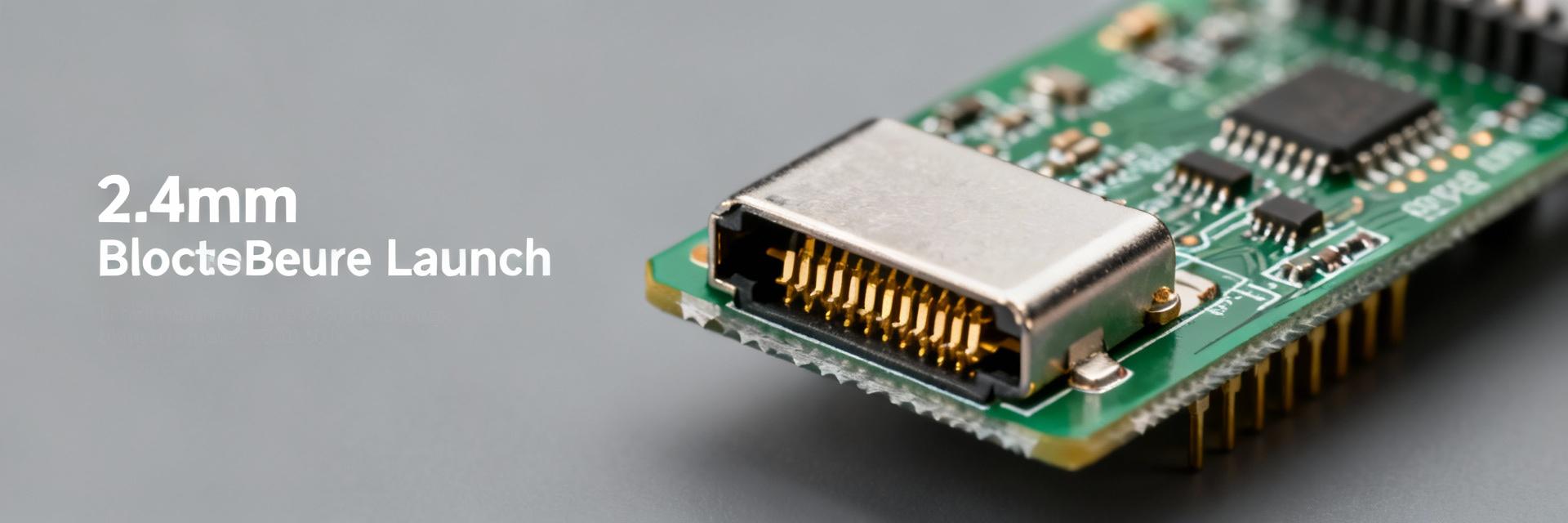
1.1 End-launch vs. edge-launch vs. coplanar launches
Point: Choosing the correct physical launch style directly affects RF performance and manufacturability. Evidence: End-launchs typically offer a short, controlled transition and are common for bench test connectors; edge-launchs integrate into board edges for minimal protrusion; coplanar launches maintain ground reference for higher-frequency stability. Explanation: For frequencies above ~10 GHz, coplanar or carefully tuned end-launchs usually give the best repeatable VSWR because they preserve the reference plane and avoid uncontrolled discontinuities. Actionable check: pick end-launch when you need removable/bench access and sufficient board edge clearance; choose edge-launch when board thickness and mechanical constraints require it; use coplanar launches when you must minimize radiation and maintain consistent 50 Ω across high GHz bands. (Long-tail suggestion: "2.4mm connector end-launch vs coplanar")
1.2 Connector gender, interface dimensions, and critical tolerances
Point: Gender and precise mechanical tolerances determine mating reliability and impedance continuity. Evidence: Critical dimensions include center pin location relative to board surface, barrel diameter, PCB shoulder height, and axial clearance; small offsets (tens of microns) can shift impedance and raise S11. Explanation: Inspect mating face flatness, center conductor concentricity, and shoulder seating tolerance. Acceptable ranges: center-pin offset ≤ ±0.1 mm, barrel concentricity ≤ 0.05 mm, shoulder seating tolerance ±0.1 mm. Inspection points: measure seating depth with go/no-go gauge, confirm concentricity under microscope, and verify contact spring engagement visually. These checks prevent mechanical misseating that manifests as return-loss spikes.
1.3 Materials, plating, and RoHS considerations
Point: Contact materials and platings influence solderability, reliability, and corrosion resistance. Evidence: Common constructions use BeCu or phosphor bronze contacts with nickel underplate and a thin gold flash; barrels and bodies may be brass with nickel or passivation. Explanation: Gold flash improves contact life but may inhibit wetting if plating thickness and surface finish are inconsistent. For solder points, ensure exposed solderable surfaces are properly plated (e.g., NiAu with controlled gold thickness or ENIG alternatives) and specify RoHS-compatible lead-free alloys (SAC305 or SAC405). Note: gold thickness greater than flash levels can lead to solder wetting issues — call out plating stacks in fabrication notes and request solderability test results if unsure.
2 — Key Specs & Measurements to Validate Before Mounting (Data / Validation)
2.1 Mechanical footprint and recommended PCB land pattern
Point: A verified footprint prevents assembly errors and mechanical stress. Evidence: Confirm pad sizes, keepout, mounting holes/clamps, and any screw bosses or retention features before fabrication. Explanation: Provide these checklist items to the PCB house: Gerber for top/bottom copper, solder mask, paste layers, mechanical (drill) layer with tolerances, and 3D STEP model for mechanical clearance check. Typical footprint checklist: pad diameter for barrel solder pad (match solder fillet), center pin pad diameter, board edge clearance for edge-launchs, and defined keepout of 0.5 mm around RF mating face. Long-tail keyword: "2.4mm connector PCB footprint". Include a short example table of key land dimensions (nominal values):
| Feature | Nominal | Tolerance |
|---|---|---|
| Center pin pad | 0.9 mm | ±0.05 mm |
| Barrel solder pad OD | 3.2 mm | ±0.1 mm |
| Mounting hole / screw | 2.5 mm | ±0.05 mm |
| Keepout from mating face | 0.5 mm | — |
2.2 RF performance specs: impedance, VSWR, and frequency limits
Point: Define electrical targets early to guide layout and QA. Evidence: Typical target: 50 Ω characteristic, VSWR ≤ 1.3:1 (≈ −20 dB return) across the intended band; for mmWave extensions, tighter control may be necessary. Explanation: Specify probe points for S11/S21 measurements—directly at the connector reference plane when possible. Measurement tips: use a calibrated VNA with SOLT or TRL suited to the fixture, perform time-domain gating when diagnosing localized discontinuities, and document the calibration plane on the drawing. Record baseline S-parameters for a golden sample to use in production comparison.
2.3 Thermal and soldering profile constraints
Point: Connectors differ in thermal robustness; validate profiles to avoid damage. Evidence: Lead-free alloys (SAC305) typical reflow profile: ramp to liquidus ~217–220 °C, peak 245–250 °C for 30–60 s, time above liquidus 45–60 s. Explanation: Confirm connector vendor maximum peak temperatures and recommend hand-soldering when the connector has delicate insulators or internal springs. When using reflow: use low-mass fixtures to avoid movement, add mechanical retention features (solder clamps or adhesive) before reflow, and qualify with repeated thermal cycle testing to confirm continued S11 performance after 10–20 cycles. If vendor data shows lower thermal limits, use selective soldering or hand solder to protect finishes.
3 — Solder & Launch Techniques for 2.4mm Connector PCB Mounts (Method Guide)
3.1 Soldering workflow: hand-solder, selective solder, and reflow
Point: A controlled solder workflow yields reliable mechanical and RF joints. Evidence: Recommended process: clean pads → apply flux → tack mechanical features → solder center pin → fillet barrel → inspect wetting. Explanation: For hand-solder, use a temperature-controlled iron ~320–350 °C with a chisel tip, Rosin-based flux, and SAC305 solder. For reflow, tack the connector with low-viscosity fixture adhesive or solder clamps; apply paste to barrel and center pad per paste stencil callouts; run a conservative profile with controlled ramp. Wetting checks: visible continuous fillet around barrel and full solder coverage under center pad. Long-tail keyword: "2.4mm connector hand solder technique". Use solder clamps or capture features when falling or floating of heavy connectors is likely during reflow; fixture with spring clips during selective soldering to avoid movement.
3.2 Microstrip vs. coplanar waveguide launch implementation
Point: Launch geometry determines impedance continuity and radiation behavior. Evidence: For a given dielectric (e.g., FR-4, Er ≈ 4.5), a 50 Ω microstrip trace width differs from a CPW trace width with ground clearance. Explanation: Rule of thumb examples (1.6 mm board): microstrip width ≈ 3.0 mm for 50 Ω on FR-4; CPW with 0.3 mm gap and ground on same layer may require trace width ≈ 1.2 mm. Reference vias: place reference vias adjacent to CPW ground gaps within 0.5 mm to maintain ground continuity. Show small layout example: position center-pad to launch edge, maintain 0.3–0.5 mm ground clearance for CPW, and add via stitch rows 0.8–1.0 mm apart to stabilize impedance.
3.3 Inspecting and avoiding common solder defects
Point: Early detection of defects saves rework time. Evidence: Common defects include cold joints (dull surface, lack of fillet), solder wicking (solder drawn up barrel reducing fillet), insufficient fillet (mechanical weak), and tombstoning (uneven solder wetting). Explanation: AOI criteria: continuous fillet, solder fillet height ≥ 0.2 mm, no bridging, and center pin fully wetted. X‑ray can show hidden voids under barrel; reflow voids > 10% area may be cause for rework. Rework best practice: remove solder with braid and re-solder with fresh flux; do not overheat connector — limit hand-solder to 10–15 s per joint and inspect after cooling.
4 — Practical PCB Layout and Manufacturing Tips (Method / Manufacturer-facing)
4.1 Via stitching, ground clearance, and EMI control
Point: Proper via placement ensures reference continuity and reduces spurious radiation. Evidence: For high-frequency launches, stitch ground near the launch with via rows 0.8–1.5 mm spacing and via diameter ≥ 0.3 mm (drill ~0.3–0.4 mm after plating) with annular ring ≥ 0.15 mm. Explanation: Place vias within 0.2–0.5 mm of the ground gap edges for CPW launches; add a staggered second row 1–2 mm out to create a controlled ground cavity. Multiple via rows reduce parallel-plate resonances and keep consistent impedance across production variance.
4.2 Example PCB stackups and dielectric choices for 50 Ω launches
Point: Stackup selection balances loss, cost, and manufacturing yield. Evidence: Example stackups:
| Stackup | Description | 50 Ω trace width (1.6 mm) | Expected loss (up to 18 GHz) |
|---|---|---|---|
| A — FR-4 standard | 1.6 mm core, 35 μm Cu | ≈ 3.0 mm (microstrip) | Moderate (higher loss past 6 GHz) |
| B — Low-loss laminate | Rogers-like, Er ≈ 3.5 | ≈ 2.2 mm | Lower loss to 18 GHz |
| C — Thin dielectric multilayer | High-density, buried microstrip | ≈ 1.0–1.5 mm | Lowest loss but higher cost |
Explanation: FR-4 is cost effective for lower GHz; for consistent performance up to 18 GHz, low-loss laminates are recommended. Provide anticipated insertion loss figures in procurement notes for EMS quoting.
4.3 How to communicate requirements to your EMS partner
- Technical Features of PMIC DC-DC Switching Regulator TPS54202DDCR
- STM32F030K6T6: A High-Performance Core Component for Embedded Systems
- APT50GH120B Datasheet Deep Dive: Specs, Ratings & Curves
- APT50GH120BSC20 Power Module: Latest Performance Report
- APT50GH120BD30 IGBT: How to Maximize Efficiency for EV Drive
- GTSM20N065: Latest 650V IGBT Test Report & Metrics
- CMSG120N013MDG Performance Report: Efficiency & Losses
- GTSM40N065D Technical Deep Dive: 650V IGBT + SiC SBD
- NOMC110-410UF SO-16: Live Stock & Price Report
- 1757255 MSTBA 5.08mm PCB: Step-by-Step Install & Solder
-
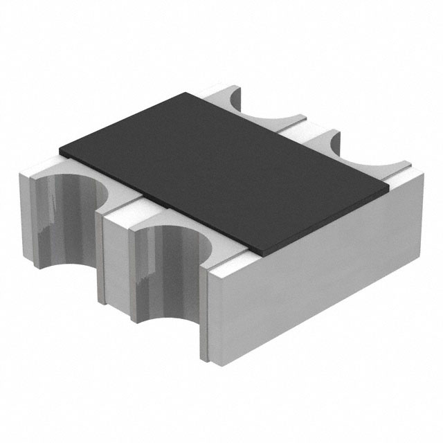 EXB-V4V120JVPanasonic Electronic ComponentsRES ARRAY 2 RES 12 OHM 0606
 -
 EXB-V4V473JVPanasonic Electronic ComponentsRES ARRAY 2 RES 47K OHM 0606
 -
 EXB-V4V823JVPanasonic Electronic ComponentsRES ARRAY 2 RES 82K OHM 0606
 -
 EXB-V4V151JVPanasonic Electronic ComponentsRES ARRAY 2 RES 150 OHM 0606
 -
 EXB-V4V181JVPanasonic Electronic ComponentsRES ARRAY 2 RES 180 OHM 0606
 -
 EXB-V4V331JVPanasonic Electronic ComponentsRES ARRAY 2 RES 330 OHM 0606
 -
 EXB-V4V152JVPanasonic Electronic ComponentsRES ARRAY 2 RES 1.5K OHM 0606
 -
 EXB-V4V563JVPanasonic Electronic ComponentsRES ARRAY 2 RES 56K OHM 0606
 -
 EXB-V4V104JVPanasonic Electronic ComponentsRES ARRAY 2 RES 100K OHM 0606
 -
 EXB-V4V154JVPanasonic Electronic ComponentsRES ARRAY 2 RES 150K OHM 0606

