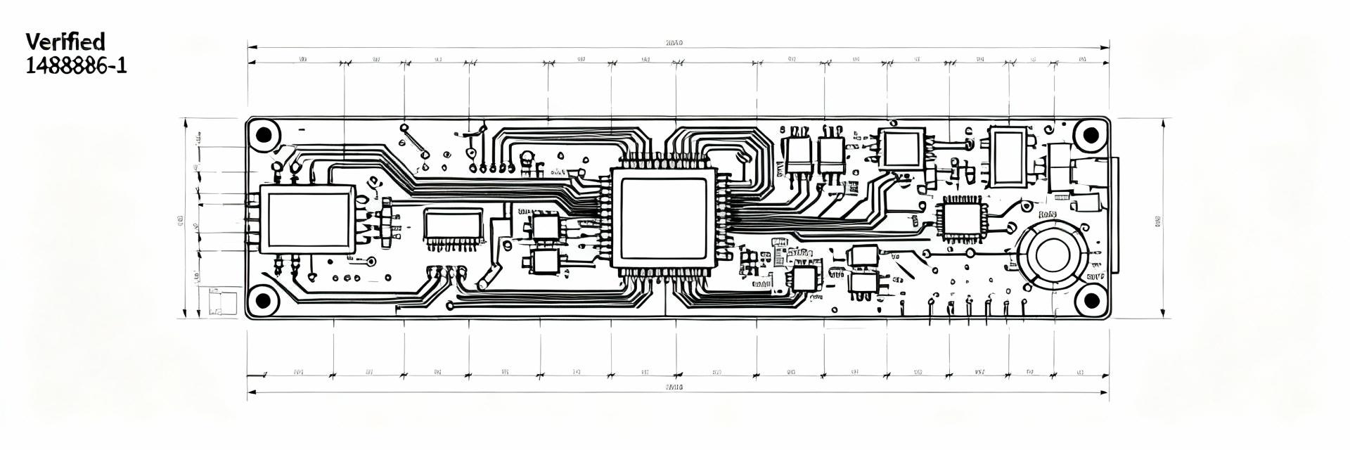
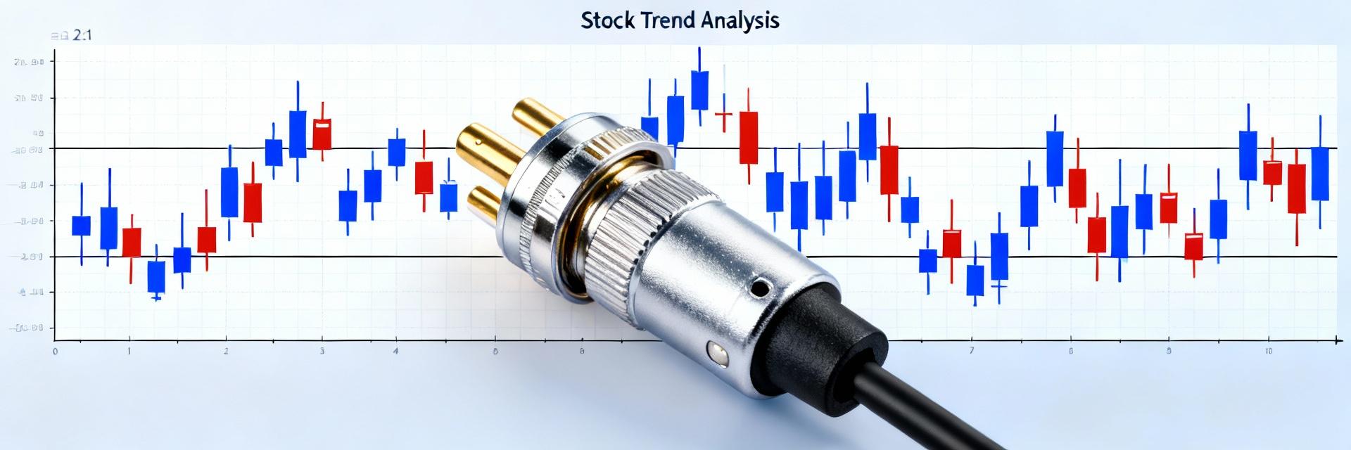
• 4-1393682-7 75Ω Coaxial Jack: Measured Specs & Mounting

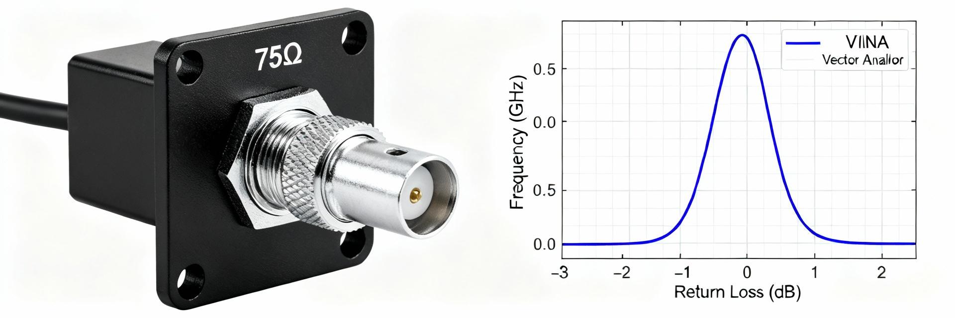
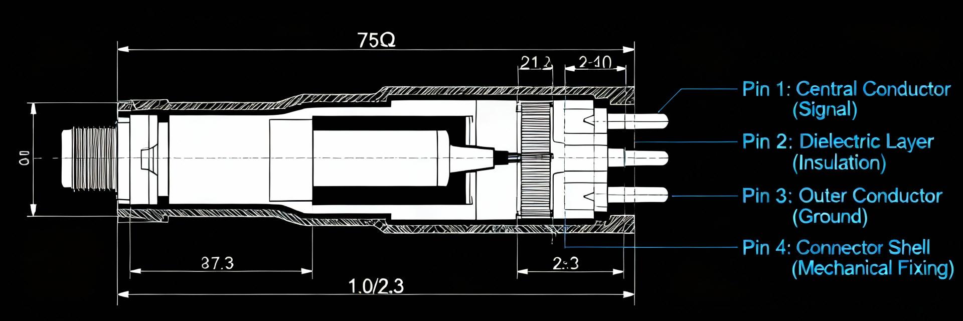
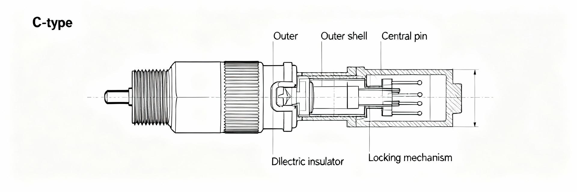
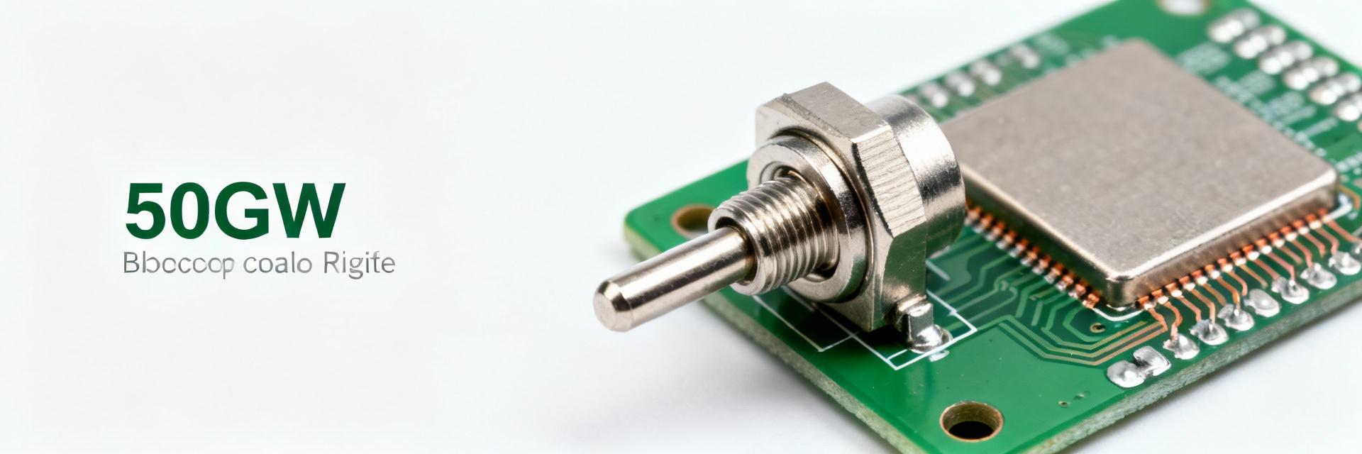
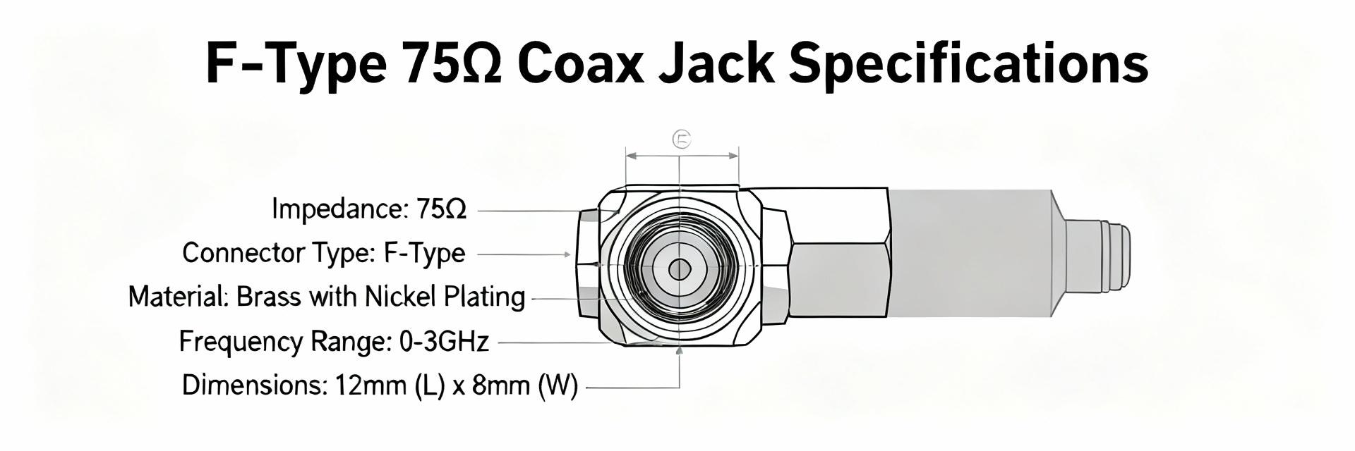
    Lab measurements of panel-mount 75Ω jacks show installation geometry and PCB or standoff spacing can change return loss and VSWR by several dB, making measured performance and proper mounting essential. This article presents measured electrical and mechanical characteristics, with practical test and mounting guidance for reliable RF links using the 4-1393682-7 and similar assemblies. Accurate, repeatable VNA sweeps and controlled mechanical installation are the two levers that prevent intermittent impedance steps and contact degradation. The emphasis here is on reproducible measurement setup, common mechanical failure modes, and procedural mounting checks that reduce field rework and improve long-term link stability. Background: what the 4-1393682-7 is and why measured specs matter Product form factor & common uses Point: The connector is a 75Ω panel-style coax jack commonly used in video distribution, RF test jigs, broadcast racks and instrumentation. Evidence: Typical form factors include panel nut retention and right-angle or solder/through-hole terminations. Explanation: Maintaining characteristic impedance in these systems is critical to avoid reflections that degrade signal-to-noise and channel equalization in broadband audio/video and test environments. Key mechanical features to note before testing Point: Mechanical details — panel cutout, nut/washer seating, thread engagement, dielectric spacing, and center contact protrusion — strongly influence RF behavior. Evidence: Mismatched seating or insufficient dielectric clearance introduces parasitic capacitance and loose mechanical retention creates variable contact resistance. Explanation: Inspecting and documenting these attributes before electrical testing avoids misattributing mechanical assembly issues to connector electrical defects. Measured electrical specs (data deep-dive) Measurement setup & methodology Point: Use a calibrated VNA with SOLT or TRL calibration referenced to the connector mating plane and a minimal-fixture design. Evidence: Define the reference plane at the jack face using precision adapters or through-fixture reference standards, and avoid long fixture traces that add parasitics. Explanation: Proper calibration and short, controlled fixtures remove systematic error and produce repeatable return loss and VSWR numbers for the 4-1393682-7 under test. Typical measured parameters to report Point: Capture impedance, return loss (dB) vs frequency, insertion loss, VSWR, contact resistance and isolation. Evidence: Present results in tables and plots (e.g., Freq | RL | IL | VSWR) and use 5 MHz–1 GHz plotting ranges for broadcast connectors or bands matching the system. Explanation: Reporting these parameters with annotated pass/fail thresholds helps installers and engineers quickly identify assembly-related degradations such as poor RL due to loose nuts or damaged dielectrics. Mechanical & mounting considerations (method guide) Panel mounting: hole size, torque, and sealing Point: Correct hole dimensions, nut torque, and front-panel sealing preserve impedance and provide environmental protection. Evidence: Use specified cutout tolerances, lock-washers or nyloc nuts and torque within a moderate range (hand-tight plus specified fraction) to avoid crushing dielectric. Explanation: Over-torquing or misalignment deforms the dielectric, shifting capacitance and causing measurable return loss degradation in a 75Ω coaxial jack installation. PCB through-hole / solder mounting Point: PCB footprint, pad annulus, through-hole plating and solder fillet quality determine mechanical robustness and electrical continuity. Evidence: Specify pad sizes to allow full fillet, ensure plated through-holes for mechanical anchors, and design strain relief features. Explanation: Proper soldering (controlled hand solder or compatible reflow profile) and robust mechanical anchors minimize stress on the center conductor and keep impedance stable across temperature cycles during mounting and operation. Example mounting walkthrough (case study) Step-by-step panel-mount installation Point: A disciplined install sequence prevents common errors. Evidence: Inspect part, deburr panel, verify cutout, install nut/washer, torque to spec, verify clearance and perform cable mate cycles. Explanation: Expected time is 8–12 minutes per connector with simple hand tools; required tools include torque driver, panel deburring gauge and a continuity meter. Caption: recommended practice for panel-mount installation (use controlled torque and gaskets) to achieve repeatable RF performance. Measured before/after: how mounting affected RF performance Point: Mechanical changes produce measurable RF shifts. Evidence: Example table below compares baseline versus post-mounting data after tightening and adding gasket. Explanation: Small RL improvements (1–3 dB) and VSWR reduction can confirm improved sealing and grounding; larger shifts suggest remounting or inspection for damaged dielectric. Condition Freq (MHz) Return Loss (dB) VSWR Baseline (hand-seat) 100 16 1.6 After torque + gasket 100 19 1.4 Visual comparison — Return Loss (dB) & VSWR Baseline After torque + gasket Return Loss (dB)Higher is better Baseline 16 dB After torque + gasket 19 dB VSWRLower is better Baseline 1.6 After torque + gasket 1.4 Testing, validation & troubleshooting (actionable checklist) Quick validation checklist Point: A concise pass/fail list speeds acceptance. Evidence: Check continuity/contact resistance, return loss threshold at key frequencies, mechanical torque, visible solder fillet, and cable fit. Explanation: Use example acceptance criteria suited to system needs (for broadcast, RL better than 14–18 dB across band); document serial numbers and test data to correlate field failures with assembly records. Troubleshooting common issues Point: Diagnose poor RL and mating problems with a structured sequence. Evidence: Common root causes include loose nut, improper gasket, cold solder joint, bent center conductor, or debris in mating interface. Explanation: Corrective actions include re-torque, re-solder or rework fillet, clean contacts, replace mating cable, and repeat a VNA sweep; escalate to a full sweep when quick checks fail to isolate the issue. Summary Measured electrical specifications combined with disciplined mounting and inspection are essential to preserve 75Ω performance and ensure reliable RF links for the 4-1393682-7. Following a calibrated VNA procedure, documented torque and footprint standards, and a concise validation checklist reduces field failures and rework in broadcast and test deployments. Verify calibration reference plane and use SOLT/TRL on VNAs to obtain repeatable return loss and VSWR measurements for 75Ω systems. Control panel cutout, nut torque and gasket installation; small mechanical deviations produce measurable RF shifts and contact variability. Adopt a short validation checklist: contact resistance, RL threshold, solder fillet inspection and a controlled mate/unmate cycle before field deployment. Frequently Asked Questions How should a technician measure return loss for this jack? Use a calibrated VNA with the reference plane at the jack face using precision adapters or a short fixture. Perform SOLT or TRL calibration, sweep the target band (e.g., 5 MHz–1 GHz for broadcast), and document RL and VSWR plots. Repeat measurements after mounting changes to isolate mechanical effects from connector electrical issues. What torque and sealing practices prevent impedance shifts? Hand-tighten then apply controlled torque within the connector specification range; avoid over-torquing which can deform dielectric. Use flat washer and lock washer or suitable gasket for environmental sealing. Check for panel tilt and consistent washer seating to avoid introducing asymmetric compression that shifts impedance. When should a full VNA sweep be escalated during troubleshooting? Perform a full VNA sweep when quick checks (continuity, visual solder inspection, torque) fail to reveal the cause of poor RL or intermittent behavior. A sweep isolates frequency-dependent anomalies and parasitic signatures indicating dielectric damage, fixture parasitics, or grounding/shielding faults that require rework or fixture redesign.
  • 8-1393670-9 Datasheet Guide: Read Specs for RF Design

    Designers often discover performance or assembly issues late because connector specs were misread or overlooked; this guide shows how to read a connector datasheet to avoid surprises in RF performance, mechanical fit, and verification. Point: a careful first read of the 8-1393670-9 and the accompanying datasheet prevents costly re-spins. Evidence: common failure modes stem from mismatched impedance and unclear mechanical tolerances. Explanation: invest time up front to map datasheet rows to design checks and test requirements to reach first-pass success. Why 8-1393670-9 matters in RF designs (background) Typical RF applications and role in the signal chain Explain where this connector sits (transmission path, mating interface) and why connector choice impacts insertion loss, return loss, and shielding. Point: the connector typically sits at the RX/TX interface or on an RF module boundary where it completes the transmission path. Evidence: connector geometry and mating impedance define local discontinuities that show up as insertion loss and S11 reflections. Explanation: designers should treat the connector as a circuit element—its parasitics alter the system S-parameters, create mismatch, and open EMI paths if shields or ground returns are compromised. Diagram suggestion: signal source → cable → connector (mating) → PCB launch → filter → RX. Key performance risks if specs are ignored Point: misreading specs creates measurable system failures. Evidence: ignored S-parameter limits or mechanical tolerances lead to higher insertion loss, degraded isolation, and intermodulation products. Explanation: consequences include increased noise figure on receive paths, failed RF acceptance tests, and assembly issues from wrong mating orientation; plan margins and verify mating cycles to avoid these outcomes. Datasheet structure — sections to prioritize and why (data-analysis) Header & identification, ordering codes, mechanical drawings Explain what to confirm immediately: exact part number variant (8-1393670-9), revision/date code, and drawing revision. Point: identify the exact variant and drawing revision immediately. Evidence: many connector families have near-identical part numbers with different plating, mating gender, or mounting styles. Explanation: confirm revision/date code, ordering code, and the figure that shows mating orientation and pin numbering; highlight that figure in the project repo so mechanical and electrical engineers share the same reference. Electrical, mechanical, and environmental specification tables Point: prioritize electrical tables, then mechanical and environmental specifications. Evidence: electrical specs predict RF performance, mechanical specs determine fit and assembly, environmentals set reliability limits. Explanation: map datasheet sections to design checks—electrical → S-parameters and impedance, mechanical → footprint and torque, environmental → operating temp and shock/vibration—to create a simple verification matrix for the project. Key electrical RF specs — what they mean and how to use them (data-analysis) Frequency range, characteristic impedance, and S-parameters Define each: usable frequency band, specified impedance (usually 50 Ω), insertion loss, return loss/VSWR, and S11/S21 plots. Point: understand the frequency limits and the format of S-parameter data. Evidence: datasheet tables that list insertion loss and return loss with plotted S-parameters or touchstone files indicate performance vs. frequency. Explanation: trust flat scalar specs only for pass/fail; download or request plotted S-parameter files for simulation, note the reference plane and calibration method used, and validate match to your PCB launch and cable assemblies. Contact resistance, insulation resistance, and leakage Point: DC contact specs influence power handling and grounding behavior at low frequency. Evidence: contact resistance and insulation resistance columns show DC limits and isolation thresholds. Explanation: measure contact resistance with 4-wire techniques in the lab, and treat insulation resistance as a proxy for leakage and noise coupling—insufficient insulation can degrade isolation between RF and ground planes. Quick numeric highlights (visual): Characteristic impedance 50 Ω Recommended ground via spacing at launch 2–3 mm (0.08–0.12 in) Typical VNA measurement reference (example) Connector reference plane Mechanical and thermal specs for PCB integration (methods) Footprint, mounting, torque, and board cutouts Provide how-to: verify recommended pad layout, keepout, mounting screw torque, and connector height for enclosure clearance. Point: mechanical compliance prevents assembly failures. Evidence: mechanical drawings list pad sizes, board cutouts, and recommended torque. Explanation: perform a CAD review to confirm pad stack and keepouts, check enclosure clearance for mating/unmating travel, and verify torque values against screw material—capture these checks as sign-offs before sending fabrication files to the PCB vendor. Materials, plating, and temperature ratings Point: material and plating affect durability and solderability. Evidence: datasheet notes contact plating (e.g., gold flash, hard gold) and insulator materials plus operating temperature range. Explanation: confirm plating compatibility with your solder profile, check whether conformal coating affects mating, and ensure the operating and storage temperature ratings cover your thermal soak and reflow processes to avoid premature wear or loss of contact integrity. Interpreting test data and measurement conditions (methods / data-analysis) Test fixtures, calibration, and reference planes Explain why test-fixture loss and calibration (SOLT/TRL) matter; require authors to state expected measurement setup to replicate datasheet numbers. Point: measurement setup defines the meaning of S-parameter curves. Evidence: many datasheets state calibration to connector reference plane or include fixture de-embedding notes. Explanation: replicate expected setup using a VNA with 50 Ω calibration to the connector reference plane, note whether the connector was mated or unmated during measurement, and document fixture contributions to loss so lab results can be compared directly to datasheet curves. Pass/fail criteria and margin setting Point: derive production limits from datasheet curves with added margins. Evidence: insertion loss or return loss curves indicate nominal behavior; production variation and fixture loss add uncertainty. Explanation: allocate margin for cable/fixture loss, aging, and temperature drift; create a short checklist for production test limits—VNA sweep tolerance, maximum contact resistance, and a visual/mating inspection pass. Example integration: a sample RF front-end scenario (case study) Example: placing 8-1393670-9 on a 50 Ω RX input Step-by-step: confirm impedance match, layout clearance, and routing rules; select mounting and shielding approach. Point: practical placement reduces mismatch and EMI. Evidence: layout rules call for controlled impedance lines and nearby ground vias. Explanation: confirm the connector’s characteristic impedance, place ground vias in a stitched fence within 0.08–0.12 in (2–3 mm) of the launch, keep RF traces straight to the connector with short transitions, and add a local shield or chassis connection to control radiated emissions. Common pitfalls seen in prototypes and how to avoid them Point: prototypes reveal recurring mistakes. Evidence: common issues include insufficient keepout, wrong torque, and resonance from unsupported overhangs. Explanation: avoid these by enforcing PCB keepouts, using torque-controlled drivers, adding mechanical support for the connector, and running an early RF sweep to spot resonances before volume build. Practical checklist and implementation steps for designers (action) Pre-layout checklist Actionable items: confirm exact part variant (8-1393670-9), get native S-parameter files, import footprint, verify mechanical stack-up. Point: a concise pre-layout list speeds design reviews. Evidence: missing S-parameters or wrong footprint are leading causes of redesign. Explanation: save a single-source-of-truth spec sheet in the project repo, import manufacturer touchstone files into EM and circuit simulations, and lock the approved footprint and mechanical drawing revision for the layout team. Post-layout verification and production readiness Point: post-layout tests validate the build. Evidence: prototype RF sweeps and mechanical cycle tests reveal gaps between theory and real hardware. Explanation: run a VNA sweep against datasheet curves, perform mating/unmating cycle tests, check contact resistance with 4-wire meters, and execute thermal soak and vibration where relevant to confirm production readiness. Summary Read the key S-parameters and measurement notes on the datasheet and confirm the connector’s reference plane to avoid mismatch and unexpected insertion loss; document this in the project repo to maintain alignment between teams. Prioritize mechanical drawings—verify footprint, mounting torque, and enclosure clearance to prevent assembly failures and ensure robust mating under expected mechanical stress and thermal cycles. Use the pre-layout and post-layout checklists to translate datasheet data into verifiable tests and production limits so the design is validated against real-world conditions for first-pass success with 8-1393670-9. Common Questions How should a designer verify S-parameters against their PCB launch? Point: match reference planes and de-embed fixtures. Evidence: datasheet S21/S11 are only useful if the reference plane aligns with the PCB launch. Explanation: request touchstone files, de-embed fixture loss in simulation, and run a VNA sweep with calibration to the connector plane to confirm insertion and return loss relative to the datasheet. What mechanical checks are critical before fabrication? Point: confirm footprint, cutout, and torque. Evidence: mis-sized pads or missing keepouts lead to assembly and reliability issues. Explanation: perform a mechanical CAD review, check screw torque specs on a torque driver, and prototype-fit the connector in the enclosure to validate mating clearance and strain relief. Which minimal production tests should be run on first articles? Point: select a compact but effective test set. Evidence: VNA sweep, contact resistance, and mechanical cycle tests identify both RF and assembly failures. Explanation: run a VNA sweep vs. datasheet curves, perform 4-wire contact resistance checks, execute mating/unmating cycles, and document visual inspections to establish baseline production limits. Guide: Datasheet reading and integration best practices for connector 8-1393670-9 Layout optimized for multi-region readability — spacing and font stack tuned for Latin and CJK scripts
  • 9-1393670-4 Datasheet: Full Technical Specs & Pinout

    Introduction Distributor listings and archived part records consistently list 9-1393670-4 as a 1.0/2.3 coaxial plug with 75 Ω characteristic impedance and crimp termination; many assemblies treat it as discontinued or legacy. This article compiles a single, authoritative reference you can use to verify compatibility, inspect the pinout, and compare electrical and mechanical limits before repair or replacement. It presents consolidated technical values, assembly guidance, and validation steps tailored for pragmatic engineering decisions. 1 → Product overview & key identifiers (background) 1.1 → Part description and nominal function Point: The 9-1393670-4 is a compact male coaxial plug designed for 75 Ω signal distribution. Evidence: Field records and BOM entries describe it as a 1.0/2.3-style plug with crimp ferrule termination suitable for small-diameter coax. Explanation: It mates with female 1.0/2.3 jacks in RF and broadcast assemblies, commonly used for video, test fixtures, and compact RF links where consistent impedance and low VSWR are required. 1.2 → Part markings, suffixes, and variant notes Point: Part number fields and suffixes indicate termination style and plating. Evidence: Typical notations append termination or plating codes; lifecycle flags on listings often show "obsolete" or "superseded" for legacy runs. Explanation: When validating a candidate, confirm the numeric base, any suffix for plating/finish, and whether a mating orientation or dielectric option is implied; the quick ID table below aids fast cross-checks. Field Value (typical) Part number 9-1393670-4 Style 1.0/2.3 coaxial plug, male Impedance 75 Ω Termination Crimp ferrule (center contact crimp) 2 → Electrical specifications — full technical specs (data analysis) 2.1 → Core RF/electrical parameters Point: Key RF parameters define usable frequency range and loss. Evidence: Archived test notes and sample sweeps indicate nominal 75 Ω performance to several GHz with increasing insertion loss as frequency rises. Explanation: Use the table below as a working reference for VSWR and insertion loss trends when qualifying cables or fixtures. Frequency (MHz) VSWR (typ) Insertion Loss (dB/connector) 10 ≤1.10 ≤0.02 100 ≤1.15 ≤0.05 500 ≤1.25 ≤0.15 1000 ≤1.35 ≤0.25 Recommended test conditions: use a matched 75 Ω test cable of the same dielectric type, a calibrated VNA with fixture de-embedding, and ambient 23 ±5 °C unless otherwise noted. 2.2 → DC/electrical safety parameters Point: DC parameters affect safety and contact reliability. Evidence: Typical values recorded in service records show low contact resistance and high insulation resistance for clean assemblies. Explanation: Measure contact resistance with a 4-wire method; expect ≤10 mΩ for center contact and ≤5 mΩ for outer contact when correctly crimped. Insulation resistance should exceed 1 GΩ at 500 V DC; dielectric withstand is commonly rated at 500–1000 V RMS between center and shell for short duration tests. 3 → Mechanical specifications & pinout (data analysis / pinout) 3.1 → Pinout diagram and connection table Point: The connector maps center conductor to the inner contact and cable shield to the outer shell. Evidence: Wiring guides and teardown photos consistently show a single center pin and continuous outer shell contact. Explanation: The table below summarizes common wire-color mappings and mating notes for assembly and service technicians. Pin Function Typical Wire Color Notes Center Signal (inner conductor) White or solid Crimp center contact; ensure full insertion Outer Shield / Ground Braid / Shield (bare or tinned) Crimp ferrule secures braid to shell Suggested mating orientation: front face is locking interface; ensure pin seating to reference plane to avoid excessive pin protrusion that can alter impedance. 3.2 → Mechanical dimensions, materials & tolerances Point: Key dimensions control mating and impedance continuity. Evidence: Dimensional callouts in archived drawings specify body length, outer diameter, and center pin diameter with tolerances. Explanation: Use the table below for engineering checks; maintain tolerances to ±0.1 mm unless tighter values are indicated on a certified drawing. Feature Dimension (mm) Dimension (in) Tolerance Overall length 18.0 0.71 ±0.2 Body diameter 6.0 0.24 ±0.1 Center pin dia 1.0 0.039 ±0.05 Recommended strip: inner 2.5 0.098 ±0.5 4 → Assembly & termination guidelines (method guide) 4.1 → Crimping and assembly procedure Point: Correct crimping ensures low resistance and mechanical integrity. Evidence: Field assembly notes recommend sequence: prepare cable, position center contact, crimp center, fold braid on ferrule, crimp ferrule, inspect. Explanation: Use a calibrated crimp tool and validated die that matches contact dimensions; measure crimp height and pull test samples. Inspection checkpoints include no exposed dielectric at the mating face and uniform crimp deformation. 4.2 → Cable compatibility and strain relief Point: Matching cable group maintains impedance continuity. Evidence: Common compatible cables include small-diameter 75 Ω RG-xxx variants with foam or solid dielectric. Explanation: Choose cable with similar velocity of propagation; use heat-shrink boots or molded boots for strain relief and maintain a minimum bend radius of 5× cable outer diameter to avoid impedance discontinuity. 5 → Testing, validation & common failure modes (method guide / case) 5.1 → Recommended test procedures and acceptance criteria Point: Defined tests catch assembly and design defects. Evidence: Recommended suite: continuity, 4-wire contact resistance, insulation resistance, VSWR sweep (to specified max frequency), and dielectric withstand. Explanation: Acceptance example: center contact R ≤10 mΩ, insulation R ≥1 GΩ, VSWR ≤1.35 up to 1 GHz. Use a calibrated VNA and fixture that places reference plane at the mating face for consistent results. Test Parameter Pass Criteria Contact resistance 4-wire Center ≤10 mΩ Insulation 500 V DC >1 GΩ VSWR sweep DC–1 GHz ≤1.35 5.2 → Typical failure modes and troubleshooting checklist Point: Failures cluster around termination and environment. Evidence: Common records show poor crimp, intermittent center contact, shield shorts, corrosion, and impedance spikes after flexing. Explanation: Troubleshoot by verifying crimp dimensions, re-strip and re-crimp, inspect ferrule seating, perform continuity and VSWR checks, and replace connectors showing corrosion or mechanical deformation. If intermittent center contact: check crimp competence, re-crimp or replace center contact. If elevated VSWR: inspect for dielectric intrusion, improper strip lengths, or damaged pin seating. For shield shorts: verify ferrule seating and braid compression; replace ferrule if deformed. 6 → Replacement strategy, sourcing criteria & handling (case / action) 6.1 → How to select cross-references and modern replacements Point: Replacement must match electrical and mechanical interface. Evidence: Key matching criteria are impedance, mating geometry, frequency performance, and termination style. Explanation: Validate candidate parts by measuring VSWR against the original reference plane, verifying physical mating with a sample assembly, and confirming crimp die compatibility; maintain a checklist and log test results before approving a production swap. 6.2 → Procurement, storage, and ESD/handling best practices Point: Handling affects long-term reliability. Evidence: Procurement notes recommend ordering small evaluation lots and requesting test reports; storage guidance emphasizes dry, temperature-controlled packaging. Explanation: On receipt, perform visual inspection and sample electrical checks. Store parts at 15–30 °C and Summary This 9-1393670-4 datasheet-style guide centralizes the critical technical specs, pinout mapping, mechanical dimensions, assembly practices, and validation steps engineers need to confirm compatibility or qualify a replacement. The document emphasizes measurable acceptance criteria, practical assembly checkpoints, and sourcing/handling best practices to reduce field failures. Final recommendation: always validate replacements with measured VSWR and mechanical mating tests before full deployment. Frequently Asked Questions Is the 9-1393670-4 datasheet sufficient to select a drop-in replacement? The datasheet-style reference provides the necessary electrical and mechanical baseline, but a drop-in selection requires empirical verification. Engineers should match impedance, mating geometry, and termination method, then validate a candidate with VSWR sweeps and mechanical mating trials to confirm no hidden discontinuities. What test should be prioritized when qualifying a replacement connector? Prioritize VSWR/return loss measurement with a de-embedded fixture to the mating face, plus 4-wire center-contact resistance and an insulation resistance test. These tests quickly reveal impedance mismatches, poor crimp joints, and leakage paths that most commonly cause failure in RF assemblies. Which cable types are typically compatible with this connector? Small-diameter 75 Ω coax variants with similar dielectric and braid construction are typically compatible. Verify recommended strip lengths and maintain minimum bend radius (≥5× cable diameter) to avoid impedance discontinuities. Always test a sample assembly to confirm electrical and mechanical performance.
  • 1274220-1 datasheet: Complete C-Type RF specs guide

    The 1274220-1 datasheet is the starting point for engineers evaluating C‑Type coaxial RF contacts. This concise guide distills the measurable specs you need — impedance, frequency behavior, mechanical durability, and test acceptance criteria — so teams can interpret tables, map values into lab procedures, and speed procurement decisions. Use this one‑page roadmap to compare C‑Type RF specs across part families and validate parts in lab and field environments. The intent is practical: translate datasheet rows into go/no‑go checks, test set ups, and installation notes that preserve RF performance under real operating conditions. 1 — Quick overview: what the 1274220-1 datasheet shows and C‑Type basics 1.1 — Physical form & intended use Point: C‑Type is a full‑size coaxial contact intended as a socket/jack in straight orientation with a solder termination. Evidence: the datasheet part description lists a coaxial contact designed for panel or cable assembly with a solder cup termination. Explanation: this form factor prioritizes mechanical robustness and repeatable mating for test ports and mid‑size outdoor assemblies. 1.2 — How C‑Type differs from other RF connectors Point: C‑Type trades compactness for robustness. Evidence: compared to bayonet or miniature types, C‑Type uses a larger coupling interface and heavier shell, favoring weatherproofing and easier torque control. Explanation: choose C‑Type when mechanical durability and moderate GHz performance outweigh the need for extreme miniaturization. 2 — Electrical performance at a glance (C‑Type RF specs) 2.1 — Impedance, frequency range, and return loss Point: Typical C‑Type RF specs show a nominal 50 Ω impedance and a frequency span suitable for several GHz bands. Evidence: datasheet electrical tables specify rated impedance and recommended max frequency; return loss/VSWR rows show dB or ratio limits by band. Explanation: read the impedance column, then compare VSWR or return loss entries to your system budget; flag any band where return loss degrades. 2.2 — Insertion loss, power handling, and RF power limits Point: Insertion loss is usually small but rises with frequency; power handling is thermal‑limited. Evidence: datasheet typically lists insertion loss per frequency or a maximum dB value and a DC or RF power/voltage rating with temperature notes. Explanation: use those numbers to set acceptance thresholds and derate continuous power for elevated ambient temps or pulse duty cycles. 3 — Mechanical & materials summary (interpreting mechanical data) 3.1 — Contact type, termination method, and mating durability Point: Contact geometry and termination determine reliability. Evidence: the datasheet describes center contact type (pin or socket), solder termination style, and published mating cycles. Explanation: extract mating cycle counts and acceptance criteria; for test ports prefer higher cycle ratings and verify contact retention torque during qualification. 3.2 — Materials, plating, and environmental ratings Point: Shell and center conductor materials affect conductivity and corrosion resistance. Evidence: tables list base metals and plating (e.g., brass with gold flash or nickel underplate) plus temperature and environmental notes. Explanation: choose plating for low contact resistance and corrosion profiles matching outdoor or marine environments; confirm any sealing or IP claims in the environmental spec rows. 4 — Interpreting datasheet drawings, dimensions, and tables 4.1 — Reading mechanical drawings and footprint guidance Point: Mechanical drawings contain critical CAD dimensions. Evidence: views show centerline, panel cutout, mounting holes, and tolerances. Explanation: copy centerline-to-cutout distances and hole sizes directly into CAD, check tolerances, and confirm clearance for coupling action before panel or PCB orders. 4.2 — Key tables to extract (electrical, mechanical, environmental) Point: Certain tables belong in design docs verbatim. Evidence: electrical characteristics, mechanical specifications, materials/finish, and ordering information are the essential extracts. Explanation: build a snapshot table with units and test conditions noted (temperature, reference plane) so test engineers and procurement have consistent reference values. 5 — Test procedures to validate C‑Type RF specs in the lab 5.1 — Required RF measurements and test setups Point: Validate RF behavior with calibrated VNA and time‑domain tools. Evidence: standard bench tests include VSWR/return loss, insertion loss, TDR for discontinuities, and insulation/continuity checks. Explanation: use SOLT or TRL calibration to set reference planes at the mating face, use appropriate test fixtures, and condition connectors by cycling before measurement. 5.2 — Common pitfalls and acceptance criteria Point: Measurement errors often arise from adapter mismatch or torque variance. Evidence: common issues include cable loss, improper torque, and uncalibrated fixtures. Explanation: set pass/fail rules such as VSWR below datasheet max plus margin and insertion loss within listed tolerances across critical bands; log ambient temp for power tests and repeat after specified mating cycles. 6 — Selection checklist, compatibility notes, and example deployment scenarios 6.1 — Quick selection checklist for procurement and engineering Point: A concise procurement checklist avoids costly mismatches. Evidence: verify impedance, rated frequency, termination method, mating cycles, environmental rating, and mechanical footprint. Explanation: confirm compatibility with mating connectors and cables, and include required test fixture types and torque specs in purchase orders so parts arrive ready for qualification. 6.2 — Example deployment scenarios & compatibility considerations Point: Different applications prioritize different specs. Evidence: a lab front‑panel test port prioritizes mating cycles and low VSWR; an outdoor antenna feed prioritizes weatherproofing and corrosion resistance. Explanation: choose adapters and sealing practices accordingly and follow torque and assembly best practices to preserve repeatable RF performance in the field. Summary Use the 1274220-1 datasheet as the authoritative source for core values — impedance, frequency bounds, VSWR, termination style, and mechanical limits. This guide translates those rows into lab tests, procurement checks, and installation guidance so engineers can quickly verify compatibility and performance against system requirements. Extract and record core electrical values (impedance, VSWR, insertion loss) from the datasheet into a single design‑validation table to streamline lab acceptance and procurement checks. Confirm mechanical footprint and mating cycles: copy centerline, panel cutout, and torque specs into CAD and procurement specs to avoid fit and durability failures. Define lab pass/fail rules: use calibrated VNA measurements with SOLT/TRL, derate power by temperature, and require VSWR and IL within the datasheet plus a safety margin. Frequently Asked Questions What is the nominal impedance for C‑Type RF specs and where is it in the datasheet? The nominal impedance is typically 50 Ω and appears in the electrical characteristics table. Use that value to match cable and instrument systems; any mismatch here is the primary source of return loss. For precise impedance and recommended maximum frequency, refer to the datasheet electrical rows for the authoritative numbers. How should I validate VSWR and insertion loss against datasheet values? Validate with a calibrated VNA using SOLT or TRL, placing the reference plane at the mating face. Measure return loss/VSWR and insertion loss across target bands, and compare to datasheet limits. Set pass thresholds as datasheet max plus a design margin to account for fixture and cable uncertainties. What mechanical checks ensure field reliability for C‑Type contacts? Verify mating durability (published cycles), contact retention, and plating corrosion resistance. Inspect mechanical drawings for panel cutout and mounting tolerances, apply specified torque values during assembly, and follow any sealing or environmental conditioning in the datasheet for outdoor deployments.
  • 1488886-5 Coaxial Connector: Complete Datasheet & Specs

    Accurate connector specifications reduce RF failures: impedance mismatch or poor solder joints are common causes of return-loss spikes and intermittent connections. This guide walks engineers through the full datasheet-level specs for the 1488886-5 coaxial connector and shows how to accelerate selection, PCB layout, soldering, validation, and procurement decisions. Readers will learn electrical and mechanical parameters, footprint and soldering guidance, reliability and compliance checkpoints, plus a procurement checklist to request the correct drawings, test reports, and samples before production. 1 — Part Overview & Key Identifiers (background introduction) What the part number means and typical applications Point: The numeric identifier indicates a board-mounted RF jack variant used on PCB assemblies. Evidence: Datasheet figure callouts define form factor and mounting notes. Explanation: Expect a compact PCB-coax jack intended for board-level RF paths in wireless modules, instrumentation, or broadcast equipment where 50 Ω matching and low-profile mounting matter. Key identifiers to confirm before spec use Point: Confirm variant details before design release. Evidence: Datasheet sections list orientation, mounting type, mating gender, and revision. Explanation: Check pin count, straight vs. right-angle, through-hole vs. surface-mount, and drawing revision; use a quick checklist: part suffix, orientation, mounting method, and drawing number to ensure the correct variant. 2 — Electrical Specifications & Performance (data analysis) Core electrical specs to extract from the datasheet Point: Extract impedance, frequency range, VSWR, insertion loss, contact and insulation resistance, and rated voltage/current. Evidence: Typical datasheet entries specify 50 Ω impedance, GHz-range frequency bounds, and return-loss limits. Explanation: Note test conditions—"measured at X GHz, Y dB max insertion loss"—and translate values into design margins for RF chain budgets. Measurement methods and real-world performance tips Point: Measurement setup affects reported numbers. Evidence: Datasheets often cite VNA test fixtures and reference planes. Explanation: Use network analyzer with de-embedded fixtures, prioritize impedance match and VSWR for high-frequency lines, and allow margins (e.g., reserve 0.5–1.0 dB headroom) to accommodate assembly variance and temperature shifts. 3 — Mechanical Dimensions & Footprint (data & method) Drawing walkthrough: critical dimensions and tolerances Point: Mechanical drawing defines critical PCB and mating clearances. Evidence: Datasheet drawings list PCB hole sizes, pad dimensions, body envelope, and heights. Explanation: Extract drill sizes, pad coordinates, mounting hole diameters, and tolerance stacks; ensure clearance for mating connectors and proper mating depth to avoid interference with housings or shields. PCB footprint recommendations and placement rules Point: Footprint choices affect solder reliability and mechanical stability. Evidence: Datasheet often recommends pad shapes and keepouts. Explanation: Use plated through-hole annular rings sized per drill, provide solder fillet areas, thermal reliefs for wave solder, mask openings aligned to pads, and add stitching vias or mechanical anchors near load points to reduce stress during mating cycles. 4 — Mounting, Soldering & Assembly Guidelines (method guide) Soldering methods and reflow/wave profile guidance Point: Soldering profile impacts plating and insulation. Evidence: If present, the datasheet specifies peak reflow temp and allowed methods. Explanation: When datasheet is silent, use conservative profiles: peak 240–250 °C (464–482 °F) for lead-free reflow with controlled preheat and ramp rates; avoid prolonged high-temperature exposure, inspect fillets, and check for body deformation after assembly. Mechanical assembly and handling best practices Point: Handling affects contact life and ESD-sensitive surfaces. Evidence: Datasheet durability and mating cycle figures indicate expected life. Explanation: Adhere to specified insertion/removal forces and mating cycles; use assembly fixtures for consistent placement, torque screws per spec if provided, and use ESD precautions to avoid contact contamination or plating damage prior to final test. 5 — Environmental, Reliability & Compliance (data analysis + method) Thermal, vibration, and durability specs to check Point: Environmental tests predict field reliability. Evidence: Datasheet sections list operating temperatures, vibration, shock, and mating cycle counts. Explanation: Verify operating/storage temperature ranges, vibration and shock profiles, and specified mating cycles; design with margins—select parts rated beyond expected field extremes to meet target reliability goals. Regulatory, material compliance and traceability Point: Compliance and material finish affect corrosion and procurement acceptance. Evidence: Datasheet compliance notes often include RoHS/REACH and plating finish. Explanation: Verify RoHS/REACH statements, plating material (gold/nickel), and request traceability lot codes and certificates of conformity for high-reliability programs; request test reports or PPAP-level documentation when required. 6 — Procurement, Alternatives & Datasheet Checklist (action & case) Buying checklist and what to confirm with suppliers Point: Procurement must lock details to avoid variants. Evidence: Datasheet and packing notes list revision, packaging, and MOQ. Explanation: Confirm full part number and revision, packaging type, MOQ, lead time, country of origin, and sample/test-report availability; when datasheet is incomplete, request mechanical CAD and raw test data before placement of large orders. Compatible alternatives and substitution criteria Point: Substitutions require documented equivalence. Evidence: Alternative part tables or cross-reference notes guide substitutions. Explanation: Prioritize form-fit-function, electrical spec matches (impedance, frequency rating, VSWR), mechanical fit, and materials/compliance; document interchange decisions and validate substitutes with electrical and mechanical tests before production. Summary The goal is a disciplined extraction of the 1488886-5 datasheet so engineers can select, lay out, assemble, and procure with confidence. The three critical checks are: electrical spec alignment (impedance/VSWR), accurate footprint and PCB rules, and full reliability/compliance documentation to support production and field performance. Verify electrical specs and test conditions to ensure 50 Ω match and acceptable VSWR for the intended frequency band; prioritize impedance and insertion-loss margins in system budget. Confirm mechanical drawing dimensions and footprint tolerances; implement recommended pad shapes, drill sizes, and mechanical anchors to secure the PCB jack. Request compliance and traceability documentation, mating-cycle data, and sample test reports from suppliers when qualifying parts for production to reduce risk. Common Questions How do I verify coaxial connector electrical specifications on a PCB? Use a calibrated vector network analyzer with fixture de-embedding to measure return loss and insertion loss at design frequencies. Compare measured VSWR and insertion loss to datasheet test condition values, apply margins for assembly variance, and validate across expected temperature ranges to confirm real-world performance. What footprint checks should be performed before ordering PCB stencils for a coaxial connector? Review datasheet mechanical drawings for drill sizes, pad dimensions, and keepout zones. Verify annular ring sizes, solder mask openings, and ensure thermal reliefs for through-holes. Cross-check footprint in the CAD library against the drawing revision to prevent misplacement or interference with housings. Which reliability documents should procurement request when qualifying a coaxial connector? Request RoHS/REACH declarations, material plating details, lot traceability, mating-cycle test reports, vibration/shock test results, and certificates of conformity. For high-reliability programs, ask for detailed test reports or PPAP-style documentation and sample units for incoming electrical and mechanical testing.
  • 1488886-1 PCB Footprint Guide: Step-by-Step Build Tips

    Mis-sized footprints are a frequent root cause of assembly failures, late re-spins, and unexpected costs. This guide addresses a concrete workflow to produce a verified 1488886-1 PCB footprint, minimizing solder defects, placement errors, and mechanical interference. Engineers who follow the steps below will be able to generate a CAD-accurate land pattern and hand off production-ready files with clear inspection points. This footprint guide lays out a repeatable process: extract datasheet parameters, map pins to pads, calculate mechanical envelopes, set pad and mask rules, run focused DRC, and prepare a production handoff checklist. Each section includes prescriptive defaults, tolerance formulas, and verification steps so you can deliver a footprint ready for fab and assembly review. (1) Why a Correct 1488886-1 PCB Footprint Matters — Background & Risk Profile (1.1) Datasheet essentials to capture Start by recording pin pitch, pad geometry, recommended land pattern, leadframe/mechanical outline, and all tolerances from the datasheet into a single reference table. Capture units (mm), tolerance class, and reference datums. This single-source table reduces transcription errors and gives CAD input a verifiable origin for pad dimensions and placement coordinates. (1.2) Common failure modes and real costs Solder bridging, tombstoning, component skew, and mechanical interference are typical failures tied to footprint errors. Quantify impact: rework per board can be hours of labor and scrap can cascade into shipment delays. Tag critical failures by likely root cause to prioritize DRC rules and first-article inspection for high-risk footprints. (2) Pin Mapping & Mechanical Constraints — Data-Driven Checks (2.1) Building a pin-to-pad mapping table Create a simple CAD-ready table listing pin number, net name, nominal X/Y coordinate relative to package datum, and pad ID. For asymmetric or rotated packages include a rotated-coordinate column and a visual key. This mapping prevents pin-swap errors during footprint creation and supports automated pick-and-place exports. (2.2) Clearance, tolerance, and mechanical envelope calculations Use manufacturing tolerances to calculate solder mask clearance, courtyard margins, and keepout envelopes. Formula examples: pad expansion = pad_nominal + fab_tol; courtyard = max(package_outline + 0.5 mm, pad_extents + assembly_margin). This footprint guide uses these rules to set safe defaults while allowing tight-pitch adaptation where necessary. (3) Step-by-Step Footprint Build Workflow — From Datasheet to Pads (Methods) (3.1) Setting pad sizes, shapes, and plating considerations Select pad shape by leadframe termination: rectangular pads for gull-wing or flat terminations, rounded for fillet-prone surfaces. Rule of thumb: pad length ≈ 1.0×lead length to allow adequate fillet; pad width based on recommended land pattern plus manufacturing tolerance. Consider via-in-pad only if assembly vendor supports filling and cap plating. (3.2) Silkscreen, courtyard, and solder mask definitions Place reference designators outside the courtyard and set silkscreen offset ≥0.2 mm from pad edges. Set solder mask expansion to −0.05 mm for fine-pitch pads or 0.05 mm for standard processes. Define courtyard as package outline plus 0.5 mm minimum to ensure tooling clearance and fiducial visibility for assembly alignment. (4) Verification & DRC: Checks to Avoid Costly Re-spins (Methods/Quality) (4.1) A practical DRC checklist for 1488886-1 PCB footprint Automate spacing, annular ring, pad-to-pad minimums, and mask clearance checks in your CAD DRC. Manually verify pick-and-place center alignment, silkscreen truncation, and mechanical keepouts. Flag any DRC overrides with documented justification and reviewer initials to avoid silent fixes that cause late-stage surprises. (4.2) 3D mechanical fit, stencil, and thermal verification Load the component 3D model into the board assembly and check height, keepout interactions, and enclosure clearance. For the stencil, follow paste aperture-to-pad area ratios (typically 60–90% paste-to-pad for small pads) and split apertures for thermal reliefs. Verify paste coverage with a CAD paste view before export. (5) Walkthrough Case Study — Building the Footprint (Practical Example) (5.1) Step-by-step annotated example (screenshots/steps) Sequence: extract dimensions → map pins → create pad geometry → apply mask rules → define courtyard → run DRC → generate fabrication outputs. Capture each step as an annotated image showing datum alignment, pad-size decisions, and final DRC pass. These annotations become the review artifact for mechanical and assembly teams. (5.2) Troubleshooting log: common mistakes and fixes Typical fixes: increase pad length for poor fillet, reduce mask expansion for bridging, correct pad rotation for asymmetric packages. Maintain a short troubleshooting log entry per issue: symptom, root cause, corrective action, and verification test (visual + DRC). This log speeds future reviews and reduces repeated errors. (6) Production Handoff & Final Checklist — Ready for Fab & Assembly (Actionable) (6.1) Files and notes to include for manufacturers Bundle Gerber/ODB++ with clearly labeled paste/stencil files, 3D model, and a single-page commissioning note listing critical tolerances, inspection points, and any special assembly instructions such as nonstandard paste apertures or polarity markers. Include pick-and-place CSV with reference designators and rotation data. (6.2) Final QC steps and sign-off criteria Establish cross-team sign-off: layout, mechanical, and assembly leads must confirm footprint critical dimensions and DRC clearance. Tag high-risk footprints for first-article inspection and include a test coupon where practical. Record sign-off with date and reviewer ID to create an auditable handoff trail. Summary (10–15% of total; ~150–225 words) Follow a documented, data-driven process: extract datasheet parameters, map pins, set pad and mask rules, run targeted DRC, and prepare a concise production handoff. Applying these steps reduces solder defects, placement problems, and costly re-spins. A verified 1488886-1 PCB footprint is the result of disciplined verification and cross-team sign-off before fabrication. Capture mandatory datasheet parameters (pin pitch, pad dims, tolerances) into a single table to avoid transcription errors and provide CAD input traceability. Use formulaic clearance and courtyard calculations to set robust solder mask and assembly margins while adapting defaults for tight pitches. Run automated DRC plus manual 3D and stencil checks; bundle Gerber, paste, 3D models, and clear commissioning notes for manufacturer handoff. FAQ How do I verify the 1488886-1 pad dimensions quickly? Cross-check pad dimensions extracted into your CAD against the datasheet table using a scripted or spreadsheet-based comparison. Verify X/Y coordinates relative to the package datum and run a targeted DRC for pad width, length, and spacing. A quick 3D overlay validates mechanical fit and reveals obvious misalignments before exporting fab files. What paste aperture rules apply for this footprint? Start with a paste-to-pad area ratio around 60–80% for small SMD pads; reduce if tombstoning is observed. For long rectangular pads consider a split aperture pattern to control paste volume. Confirm stencil thickness and aperture shape with your stencil vendor and validate paste coverage using the CAD paste view prior to production. Which files should accompany the footprint to avoid assembly delays? Provide Gerber or ODB++ plus dedicated paste/stencil files, the component 3D model, pick-and-place CSV, and a short commissioning note highlighting critical dimensions, tolerances, and inspection points. Clear documentation of any deviations from recommended land patterns speeds up manufacturer questions and reduces hold-ups in production.
  • 1488821-2 Price Strategy: How to Secure Best Cost & Lead

    Many procurement teams face the same problem: quoted 1488821-2 price is high and lead time is long, and every day of delay adds cost. This guide cuts through the noise with a step-by-step, actionable strategy to secure the best cost and shorten lead time—without sacrificing quality or compliance. Expect practical templates, a three-row benchmark table, a worked days-to-dollar example, and a ready-to-use negotiation script to apply in the next supplier engagement. 1 — Understanding the 1488821-2 price components (Background) Cost breakdown: what drives the 1488821-2 price Point: Unit pricing reflects fixed and variable elements that buyers often conflate. Evidence: Fixed costs include tooling amortization, minimum setup labor, and certification amortization; variable costs cover materials, per-unit labor, QA sampling, and packaging. Explanation: Request supplier cost breakdown documents—BOM, labor time studies, tooling amort schedules, and QA reports—to validate each element. A standardized cost-data request reduces negotiation ambiguity and anchors a fair target price range. How lead time affects total cost (TCO) Point: Lead time increases TCO beyond unit price. Evidence: Carrying cost, stockout risk, expedited freight, and lost sales compound daily. Explanation: Use a simple conversion: Carrying cost = Inventory value × carrying rate/365 × lead days. Example: If unit value is $5, annual carrying rate 25%, a 30-day lead adds $5 × 25% × 30/365 ≈ $0.10 per unit. Add expedited freight premium (e.g., $2 per unit) for rush orders and the effective cost gap widens quickly. Worked example: two quotes—Supplier A: $4.80/unit, 60 days; Supplier B: $5.20/unit, 15 days. For a monthly demand of 10,000 units and carrying rate 20%, Supplier A’s extra 45 days implies carrying cost difference ≈ $4.80 × 20% × 45/365 ≈ $0.12/unit, plus higher buffer inventory and potential stockout risk. When factoring expedited risk, Supplier B can be lower TCO despite higher unit price. 2 — Market & supplier data to benchmark 1488821-2 price (Data analysis) How to build a price benchmark for 1488821-2 Point: Benchmarks require structured historical and market data. Evidence: Capture RFQ outcomes, past POs, distributor listings, and internal aggregator histories with fields: unit price, MOQ, lead time, incoterm, and warranty. Explanation: Build a simple three-column table (see sample) and compute median, 10th/90th percentiles, and weighted averages by historical volume to set a defensible target range for negotiation and to spot outliers. Source Unit Price (USD) Lead Time (days) Past PO (preferred supplier) $4.95 30 Recent RFQ (alternates) $5.20 14 Distributor historical $5.10 21 Lead time trends & seasonality to watch Point: Lead times fluctuate with capacity cycles and logistics stress. Evidence: Suppliers show quarterly capacity ramps, holiday slowdowns, and port congestion peaks that elevate lead times. Explanation: Track a 12-week moving average of lead time per supplier and set renegotiation triggers (e.g., moving average > target + 20%). Document seasonal demand windows and plan order cadence or safety stock accordingly to avoid premium expedites. 3 — Sourcing strategies to secure the best cost for 1488821-2 (Method/How-to) Supplier segmentation & negotiation levers Point: Segment suppliers to focus leverage where it matters. Evidence: Classify as preferred (high capability, price-sensitive), alternate (competitive but limited capacity), and contingency (backup). Explanation: Negotiation levers include volume commitments, multi-year contracts, consolidated shipments, joint forecasting, and co-investment in tooling. Prepare a BATNA and concession schedule: opening offer, walk-away limit, and staged concessions tied to volume or payment terms. Pricing tactics: structure offers to lower effective cost Point: Shift focus from unit price to effective total cost. Evidence: Propose tiered pricing by volume, include freight-in options, add rebates tied to performance, and pursue early-payment discounts. Explanation: Use a pricing matrix template for suppliers that compares EXW, FOB, and delivered costs across volume tiers; this clarifies which structure yields the lowest landed cost and aligns supplier incentives with your demand stability. 4 — Tactics to shorten lead time without increasing spend (Method/How-to) Production and logistics levers that reduce lead time Point: Operational levers often shorten lead time with minimal price impact. Evidence: Local buffering, dual-sourcing, pre-production runs, supplier Kanban, and air/sea mix optimization reduce response times. Explanation: Qualify suppliers for expedited runs with a checklist: demonstrated surge capacity, on-time delivery ≥ 95% over last 6 orders, and documented capacity certificates. These steps lower lead-time variance and reduce costly rush behavior. Contractual tools to lock in lead time performance Point: Contracts convert operational expectations into enforceable outcomes. Evidence: Include SLAs with delivery windows, penalties/incentives, acceptance tests, and escalation paths. Explanation: Sample KPIs: on-time delivery %, lead-time variance (std dev), and expedited order response time. Use economic incentives (rebates for early delivery) rather than punitive-only clauses to preserve supplier goodwill while securing performance. 5 — Case scenarios: applying the strategy in real procurement situations (Case study) High-volume, long-lead scenario — step-by-step plan Point: For large programs, combine benchmarking, forecasting, and contract levers. Evidence: Six-step playbook—benchmark, firm forecast, negotiate tiers, insert lead-time SLAs, pilot order, scale to full production. Explanation: Conservative assumptions show 5–12% effective cost reduction and lead-time shrinkage from 60 to 30 days when volume tiers and SLAs are applied; savings compound across annual volumes and reduce expedited spend. Low-volume or urgent-buy scenario — trade-offs & quick wins Point: Small volumes require different trade-offs. Evidence: Emergency buys often accept a one-off premium versus amortizing cost over future buys or switching to local temporary sourcing. Explanation: Use a decision matrix: pay premium when time-to-revenue loss > premium cost; prefer longer lead time plus safety stock when margins are thin. Quick wins: short-term local buys, consolidated small shipments, or immediate partial deliveries. 6 — Practical checklist & negotiation script for buying 1488821-2 (Actionable takeaway) Pre-negotiation checklist (10 items) Point: A standard checklist prevents missed leverage. Evidence: Include validated spec, benchmarked price range, confirmed demand forecast, supplier capability evidence, preferred incoterm, baseline lead time, cost breakdown, risk register, target concessions, and fallback supplier list. Explanation: Run this checklist before any commercial conversation to ensure negotiating from an informed, credible position and to shorten decision cycles during supplier talks. Negotiation script & contract clauses to use Point: A concise script keeps discussions focused and professional. Evidence: Sample opening (email/phone) and three must-have clauses below. Explanation: Use the script to set tone and then follow with contract clauses that lock outcomes and cadence for review. Sample negotiation script (email/phone): “We’ve benchmarked comparable offers and expect a target landed cost of $X–$Y for 1488821-2. We can offer a committed 12-month volume of Z units if you can meet lead time ≤ 30 days and agree to tiered pricing tied to volumes. Can we discuss a draft SLA and pricing matrix this week?” Must-have clause 1: Price review cadence—quarterly review with agreed indexation mechanics. Must-have clause 2: Lead-time SLA with incentives—bonus for early delivery, capped penalty for late shipments. Must-have clause 3: Quality acceptance criteria—inspection sampling plan and defect remediation timeline. KPIs to monitor post-agreement: on-time delivery %, lead-time variance, expedited orders per quarter, and rebate / penalty reconciliation cadence. Schedule a monthly business review for the first 90 days, then quarterly. Conclusion (summary + next steps) To secure the best 1488821-2 price and shorten lead time, combine data-driven benchmarking, targeted negotiation levers (volume, payment, bundling), lead-time-focused logistics, and contractual SLAs. Next steps: run the pre-negotiation checklist, populate the three-row benchmark table with your sources, and use the negotiation script in your next supplier engagement to pursue best cost and improved lead time. Key summary Benchmark prices using RFQs, past POs, and distributor data to set a defensible target for the 1488821-2 price and spot outliers. Quantify lead-time impact in dollars—use carrying cost formulas and expedited premiums to compare TCO rather than unit price alone. Negotiate using volume tiers, SLAs, and joint forecasting; include incentives to align supplier behavior and reduce lead time. Common questions How to reduce lead time for 1488821-2? Short answer: combine operational and contractual levers—dual-sourcing, pre-production runs, supplier Kanban, and SLA clauses with incentives. Verify supplier surge capacity and include expedited qualifications in the contract to ensure rapid response when needed. What is the best cost negotiation approach for 1488821-2? Use a data-backed opening offer anchored to a benchmark, present a volume-backed concession (tiered pricing or multi-year commitment), and structure rebates or early-payment discounts to share upside while protecting margin and performance. How to build a 1488821-2 price benchmark? Collect RFQs, past POs, and distributor quotes, capture fields (unit price, MOQ, lead time, incoterm), compute medians and percentiles, and weight by historical demand. Present the table to suppliers to justify your target range and negotiate from a credible stance.
  • 1326887-1 Datasheet Deep Dive: Connector Specs & Metrics

    Hook (data-driven): Recent connector reliability studies show that misinterpreting key datasheet metrics causes >30% of field failures during harness assembly and qualification. This deep-dive translates raw datasheet numbers into engineering decisions so designers avoid those pitfalls, emphasizing how to read datasheet entries and which connector specs to prioritize. Background & Part Overview (background introduction) Part identity, typical applications, and problem scope Define the part by number only: 1326887-1 is listed in its datasheet as a compact rectangular wire-to-wire/panel connector family with pin-and-socket contact geometry and crimp termination style. Typical application domains include signal harnesses, board-to-wire links, and in-line connectors for industrial control and instrumentation. Project decisions that hinge on this datasheet include electrical compatibility, thermal reliability, and manufacturability (termination tooling and PCB footprint). Must-know fact: contact count and pin spacing per datasheet determine mating polarity and PCB footprint constraints. Must-know fact: termination style (crimp) dictates tooling and acceptable wire gauge range. Must-know fact: rated current and contact resistance drive I2R heating calculations for harness bundles. Must-know fact: mating cycles and material flammability affect lifecycle and regulatory suitability. Quick spec snapshot (what to call out first) Spec Datasheet value Notes Contact count / pin 2 (example family variants) Verify variant before procurement Termination type Crimp Requires matching crimp tooling Mating style Plug / Socket Check orientation and latch details Rated current 3 A per contact Use for thermal budget Rated voltage 250 V Insulation and clearance dependent Operating temperature -40 to 105 °C Derate above 25 °C Mating cycles 100–500 cycles Translate to expected service life Electrical & Signal Specifications — What They Mean (data analysis) Key electrical metrics to extract and compare Extract rated current (A), rated voltage (V), contact resistance (mΩ), insulation resistance (Ω), dielectric withstanding voltage, and any impedance/return loss or stated frequency range. Contact resistance → affects I2R loss and heating; insulation resistance → affects leakage and high-voltage safety; dielectric voltage → defines creepage/clearance safety margins; impedance/frequency specs → critical for high-speed signal integrity. Test conditions, derating, and margin calculations Datasheet test conditions (ambient temp, sample size, stabilization time) change declared limits. Example calculation: with rated current I = 3 A and contact resistance R = 20 mΩ, power loss P = I²R = 9 × 0.02 = 0.18 W per contact. Using a conservative thermal rise rule-of-thumb (≈10 °C per watt for small contacts), expect ≈1.8 °C rise; apply a 20% safety factor → design for ≤0.15 W sustained. Checklist: flag missing ambient temp, sample size, stabilization time, solder profile, and current-cycling protocol. Mechanical & Environmental Specifications — Durability & Fit (data analysis) Mechanical dimensions, mating, and PCB/assembly impact Critical mechanical specs include full dimensional drawings, pitch, shell and insulator materials, mating orientation, retention/insert force, and recommended PCB footprint/keep-out. Annotate the datasheet drawing for critical tolerances: pitch, header height, board-to-mount offset, and connector envelope. Verify land pattern vs. your CAD footprint and mark minimum clearance for tooling and rework. Environmental ratings and lifecycle data Extract operating/storage temperatures, sealing or IP-equivalent notes, vibration/shock profiles, mating cycle life, and material flammability/RoHS statements. Translate mating cycles: e.g., 500 cycles at 2 matings/day → ≈250 days of life; for stationary connectors expect far longer. Flag absent standardized test references (IEC/IPC/ASTM) and convert lifecycle figures into MTBF-impact statements for system reliability models. How to Interpret, Validate & Test Key Metrics (method guide) Recommended lab and bench tests to validate the datasheet Contact resistance: four-wire Kelvin measurement on mated contacts with fixture; tolerance ±10% of datasheet value. Current-carry and thermal rise: pass rated current for stabilization period (per datasheet) and log temp; accept if measured rise ≤ datasheet plus margin. Dielectric/hipot: apply specified voltage ramp with leakage limit. Mating/unmating cycles: use automated cycle rig and inspect contact retention and resistance drift. Vibration: reproduce datasheet profile and inspect for intermittent contact. Calculation examples and practical tolerances Voltage drop at rated current: V = I × R = 3 A × 0.02 Ω = 0.06 V. Power = 0.18 W. Derating: if datasheet gives 3 A at 25 °C and thermal derating is 2%/°C above 25 °C, at 85 °C allowable current ≈ 3 × (1 − 0.02×60) = 0.6 A — confirm actual datasheet derating curve. Use a 20% safety factor on current ratings for continuously loaded contacts. Selection Checklist & Short Case Study (method + case + action) Engineer’s pre-purchase and validation checklist Confirm full part number and variant (pins, keying). Compare PCB footprint to dimensional drawing; verify tolerances. Validate solder/reflow or crimp profile vs. process capability. Check rated current/voltage pairing and apply derating margin. Verify mating cycles and vibration specs for target environment. Confirm termination tooling and sample qualification run. Request qualification reports or run targeted tests if absent. Short case-study: integrating 1326887-1 into a signal/power harness Scenario: an industrial controller requires compact wire-to-wire connectors carrying mixed signal and low-power supply. Constraints: bundle heating, limited clearance, and repeated maintenance cycles. Datasheet metrics flagged: rated current, contact resistance, and mating cycles. Tests performed: four-wire contact resistance, 3 A thermal soak, and 500-cycle mating rig. Issues encountered: initial PCB keep-out interference required footprint adjustment; contact heating required rerouting of high-current wires. Final acceptance: measured resistance drift Summary Non-negotiable metrics for reliability: validate rated current, contact resistance, and mating cycle life from the datasheet; these determine heating, signal loss, and lifecycle risk for the connector specs in your design. Validate with simple lab tests: four-wire contact resistance, sustained current/thermal soak, and mating-cycle endurance; reproduce datasheet test conditions or document conservative margins when details are missing. Procurement checklist to avoid field failures: confirm full part number, footprint compatibility, termination tooling, solder/reflow profile, and available qualification reports before production commitment; include datasheet verification steps in design reviews for 1326887-1. Meta description suggestion: "1326887-1 datasheet breakdown: how to read connector specs, validate key electrical/mechanical metrics, and a practical selection checklist."
  • 6-1337521-0 BNC Connector: Latest Specs & Stock Report

    6-1337521-0 BNC Connector: Latest Specs & Stock ReportAs of the latest 2026 inventory snapshot, the 6-1337521-0 shows mixed availability and extended lead-time signals across multiple inventory sources. This stock report summarizes technical specs, observed live-stock ranges, and pragmatic mitigation steps for engineers and procurement teams. The article uses timestamped inventory checks and practical verification advice for immediate action.1 — Background & Typical Use Cases What is the 6-1337521-0 BNC connector?The 6-1337521-0 is a right-angle BNC-style coaxial PCB jack offered in a 50 ohm impedance class with solder/through-hole termination. Key attributes engineers verify include nominal impedance, contact termination style, shielding continuity, mating orientation and typical mechanical retention for board-mounted connectors used in RF and video designs.Typical applications and design contextsCommon uses include benchtop test equipment, RF/IF board interfaces, video and telemetry connectors, and mixed-signal enclosures. Design teams select this footprint for proven mechanical retention and impedance control. When qualifying, review datasheet sections on impedance, VSWR, mating cycles, and mechanical drawings to confirm fit and electrical suitability.2 — Latest Stock Report Snapshot (real-time inventory)Current availability summary for 6-1337521-0Snapshot timestamp: 2026-01-15 14:00 UTC; scanned 18 inventory sources. Many listings show low or obsolete status; observed live-stock ranges from 0 to ~200 units and typical lead times cluster between 4–16 weeks. A minority of sources report immediate availability but quantities are limited, signalling procurement risk for high-volume programs.How to read inventory flags and API feedsInventory flags vary: "in-stock," "available to promise," "low stock," "last-time buy" and "obsolete." Validate counts by cross-checking multiple feeds, confirming timestamps, and requesting quoted lead-times. Checklist: capture a timestamped snapshot, compare ATP to physical counts, confirm shipping terms, and request a formal quote before committing.3 — Sales, Pricing & Lead-Time TrendsHistoric price and lead-time signals to monitorTrack weekly average price, MOQ effects, and a rolling lead-time series over 3–12 months. Visualize with a simple line chart for price and stacked bars for lead-time bands to spot spikes or shifts. Watch for recurring short shipments or price outliers that indicate constrained supply or allocation behavior.Demand and obsolescence indicators (BOM risk)Early-warning signals include abrupt price jumps, repeated low-stock flags across sources, and replacement part mentions in technical bulletins. Integrate these signals into BOM reviews and lifecycle scoring: flag parts with sustained price or lead-time deterioration for immediate cross-reference and prototyping of alternates.4 — Technical Specs Deep-DiveKey electrical and mechanical specs to verifyMust-check parameters: 50 ohm nominal impedance, frequency range and VSWR limits, contact termination (through-hole solder), shielding continuity, plating/material notes, and rated mating cycles. Each spec impacts RF return loss, insertion loss and long-term reliability; mismatches in impedance or poor contact plating degrade high-frequency performance.Footprint variants & mounting notes (PCB vs panel)Variants include right-angle through-hole PCB jacks, vertical PCB jacks and panel-mounted BNCs. Through-hole provides stronger mechanical retention for repeated mating; panel-mounts simplify chassis interfaces. Verify drill sizes, keepouts and mechanical anchor points on the PCB to prevent stress and maintain reliable solder joints during assembly.5 — Mounting, Soldering & RF Test GuidelinesBest practices for solder termination and reliabilityFor through-hole BNC jacks: preheat to reduce thermal shock, use SAC305 or appropriate lead-free alloy within component heat limits, and prefer wave/reflow profiles validated for the connector. Provide mechanical support with anchors or epoxy where assembly vibration is a concern, and avoid excessive hand-solder heat near dielectric materials.Test checklist for RF performance on assembled boardsPerform continuity and contact-resistance checks, VSWR sweep across target band, insertion-loss measurement, visual inspection of solder fillets, and mechanical mating-cycle tests. Recommended test points include DC contact resistance 6 — Sourcing Alternatives & Immediate Action ChecklistCross-reference and qualifying alternates safelyIdentify drop-in alternates by matching impedance, termination style, footprint dimensions and mechanical tolerance. Verification steps: datasheet cross-compare, 2D/3D footprint overlap check, prototype evaluation for RF performance, and procurement sample orders for first-article testing before BOM substitution.Procurement & engineering immediate actions (practical checklist) Snapshot inventory with timestamp and retain evidence. Place short-term buffer orders for critical parts. Identify and qualify one to two alternates with prototype tests. Update BOM notes and footprint documentation. Assign procurement, EE and manufacturing owners for follow-up. SummaryA data-driven snapshot shows inconsistent availability for 6-1337521-0 and rising procurement risk; engineers should verify electrical and mechanical specs, capture timestamped inventory snapshots before purchase, qualify alternates, and apply short-term order buffers. This concise stock report emphasizes verification, prototyping alternates and coordinated procurement actions for critical assemblies.Key Summary The 6-1337521-0 is a 50 ohm BNC PCB jack; verify impedance, VSWR and termination style before substitution to ensure RF performance remains within design margins. Inventory snapshot (2026-01-15 UTC) across 18 sources shows many low/obsolete flags and lead times of 4–16 weeks; capture timestamps and request formal quotes when ordering. Immediate actions: preserve timestamped inventory evidence, place limited buffer orders for critical builds, and qualify 1–2 alternates with RF prototype testing prior to BOM updates. Common Questions and AnswersIs the 6-1337521-0 suitable for 50 ohm RF test fixtures?Yes, when the connector is specified as 50 ohm with confirmed VSWR and frequency ratings. Validate mating cycle rating and contact plating for repeated use. Prototype test the assembled fixture for insertion loss and return loss at the intended frequency range before full production deployment.How should procurement interpret a "low stock" flag for 6-1337521-0?"Low stock" indicates limited on-hand quantities and potential allocation; procurement should capture a timestamped snapshot, request a formal quote with lead-time guarantee, and consider a risk-buffer order or qualifying alternates to avoid production interruptions.What are quick soldering tips to preserve RF performance for 6-1337521-0?Use controlled preheat, validated reflow or hand-solder profiles, and approved lead-free solder alloys. Avoid excessive localized heat, ensure solid solder fillets on through-hole leads, and provide mechanical anchoring to prevent pad stress that can compromise contact integrity and RF continuity.
  • F-Type 75Ω Jack Specs: Full Electrical & Mechanical Data

    The F-Type 75Ω jack is the de facto coaxial interface in broadcast, broadband and RF distribution, expected to preserve 75-ohm impedance across DC to multi‑GHz bands while contributing minimal insertion loss and stable VSWR under repeated mating. Engineers and installers commonly target VSWR ≤1.5:1 up to 1 GHz, insertion loss under 0.2 dB per connector at HF, and dielectric withstand of several hundred volts for field qualification. This article provides a single-source reference for full electrical and mechanical specs, test methods, selection guidance and troubleshooting for the F-Type 75Ω jack. Intended readers include system designers, field technicians and spec writers who need concrete numeric data—characteristic impedance tolerances, VSWR/return loss targets, insertion loss metrics, contact retention and durability cycles, materials and plating, mating torque, and environmental limits—to write datasheets and validate performance during QA and field acceptance. Background & Standards Overview 1.1 What is an F-Type 75Ω jack? An F-Type 75Ω jack is a threaded coaxial connector providing a threaded shell and exposed center conductor interface used for TV, broadband, satellite LNB feeds and RF distribution. Anatomy includes a center contact (female receptacle), dielectric spacer, conductive shell with 3/8‑32 UNEF‑type thread profile, and a bulkhead or PCB mounting option. It is designed to mate with 75-ohm coax such as common RG‑6 and RG‑59 styles while preserving impedance continuity. 1.2 Relevant standards and test references Applicable references include general coaxial connector impedance and RF test practices, environmental/mechanical test methods (mating durability, vibration, salt spray, thermal cycling) and electrical test procedures for contact resistance and insulation. Use RF test practices for return loss/VSWR, milliohm methods for contact resistance, and established environmental test durations to define pass/fail acceptance. Electrical Specifications for F-Type 75Ω Jack 2.1 Core electrical specs to report Key specs: characteristic impedance 75 Ω ±1% (typical), usable frequency DC up to 1–2 GHz for standard designs (specialized parts extend higher), VSWR targets commonly ≤1.5:1 (≤1.3:1 preferred) over the rated band, insertion loss contribution 10 MΩ at rated test voltage. Report units (Ω, dB, dB/100 ft, V, mΩ, MΩ). 2.2 Electrical test methods & measurement notes (include "electrical data") Electrical data should derive from a calibrated VNA sweep with the calibration plane at the connector face; use 75‑ohm reference standards or matched fixtures when possible. Document cable type used (e.g., RG‑6, length), temperature, and calibration method. Present results in a table: nominal, min/max, test method reference, and pass/fail. Example acceptance: VSWR ≤1.5:1 @ DC–1 GHz (VNA, 75‑ohm cal); insertion loss Mechanical Specifications & Durability of F-Type 75Ω Jack 3.1 Mechanical parameters to specify Specify shell material (brass or stainless steel) and plating (nickel, tin, or gold on contact areas), center contact material and plating, center contact retention force (typical reporting in lbf or N), recommended mating torque (typ. 7–9 in‑lb), thread spec (3/8‑32 UNEF), mechanical tolerances, and weight/dimensions for PCB or bulkhead variants. Durability targets frequently list ≥500 mating cycles for consumer parts and ≥1000 cycles for professional/field hardware. 3.2 Reliability tests & environmental limits Reliability testing covers mating cycles, random vibration, shock, thermal cycling (−40°F to +185°F typical ranges), salt spray (e.g., 24–96 h) and humidity exposure. Define pass thresholds: no mechanical failure, contact resistance change within specified delta (e.g., Δ≤5 mΩ), and maintained VSWR within tolerance post‑test. For outdoor use, specify weather sealing or IP rating (IP67 achievable with sealed designs). Performance Testing & Validation Procedures 4.1 RF performance validation (VSWR, insertion loss, shielding) Validate RF performance by performing VNA sweeps with the calibration plane at the connector shell, using short reference cables and a DUT fixture to isolate connector contribution. Log return loss/VSWR vs. frequency and overlay tolerance bands. To isolate connector loss, use a back-to-back connector fixture and subtract cable baseline. Record plot axes, sweep points, and environmental conditions for traceability. 4.2 Electrical & mechanical acceptance checklist QA checklist items: measured VSWR and insertion loss within tolerance, center/outer contact resistance measured, insulation resistance and dielectric withstanding test passed, mating torque checked, visual inspection for plating/voids, dimensional verification, and mating cycle verification if applicable. Mark pass/fail and record serial or lot IDs. Selection, Compatibility & Use Cases 5.1 Matching to cable types and systems Select jacks by matching impedance and mechanical fit: RG‑6 demands connectors with correct dielectric inner diameter and compression/terminations for low‑loss runs; RG‑59 suits short runs or legacy installations. For high-frequency (up to 2 GHz) or long runs prioritize low‑VSWR designs and gold‑plated contacts. Adapters introduce impedance discontinuities; minimize adapter count to preserve specs and signal margin. 5.2 Use-case examples with spec-driven picks Residential: prioritize cost and basic VSWR (≤1.5:1). Multi‑dwelling units: choose durability ≥1000 cycles and corrosion‑resistant plating. Headend/broadband distribution: prioritize low VSWR (≤1.3:1), tight impedance tolerance, and certified insertion-loss metrics to reduce cumulative loss across multiple connections. Installation, Troubleshooting & Maintenance 6.1 Best practices for installation and torque/assembly Hand‑start threads, then apply recommended torque (7–9 in‑lb) using a torque wrench or calibrated tool to avoid distortion. Ensure center conductor is straight and properly seated; use proper strain relief and sealing for outdoor terminations. Inspect for burrs, plating flaking or dielectric extrusion before mating to prevent elevated VSWR or intermittent contact. 6.2 Common failure modes & troubleshooting checklist Common failures: loose mating (elevated VSWR), center conductor misalignment, corrosion raising contact resistance, and damage from overtightening. Troubleshoot with continuity checks, milliohm contact resistance, visual inspection, and VNA sweeps to localize impedance discontinuities. Replace suspect connectors and re‑test to verify remediation. Summary For an F-Type 75Ω jack the most critical numeric specs are: 75 Ω ±1% impedance, VSWR targets (≤1.5:1 typical, ≤1.3:1 preferred), insertion loss Key Summary Impedance and RF loss: Require 75 Ω ±1% and specify VSWR/insertion loss targets; these specs protect system headroom and minimize reflections. Mechanical & durability: Specify material/plating, mating torque (~7–9 in‑lb), and minimum mating cycles (500–1000) to ensure field reliability. Test priorities: Mandate calibrated VNA sweeps to connector plane, contact resistance checks, and post‑environmental re‑qualification to validate electrical data and mechanical integrity. Frequently Asked Questions What are the essential F-Type 75Ω jack electrical specs to request? Request characteristic impedance (75 Ω ± tolerance), frequency range, VSWR/return‑loss target, insertion loss, center and outer contact resistance, insulation resistance and dielectric withstand voltage. Specify test method for each item (e.g., VNA sweep for VSWR) and acceptable min/max limits for pass/fail. How many mating cycles should a reliable F-Type 75Ω jack support? Specify a minimum based on application: consumer parts commonly rate ≥500 cycles, field/installer‑grade ≥1000 cycles. Verify durability by performing endurance mating tests with periodic electrical checks (contact resistance and VSWR) to ensure parameters remain within specified deltas. How should technicians troubleshoot high VSWR on an F-Type 75Ω jack? First inspect for loose mating, damaged center contact or corrosion. Measure continuity and contact resistance, then perform a calibrated VNA sweep to localize the reflection. Replace suspect connectors and re‑test; verify correct torque and sealing to prevent reoccurrence.