-
- Contact Us
- Privacy Policy
- term and condition
- Cookies policy
How to Read 89S201-272N1 Datasheet: RF Specs Explained
Many RF engineers and PCB designers waste hours deciphering connector datasheets and miss critical specs that break prototypes. This practical guide gives a step‑by‑step method to parse the 89S201-272N1 datasheet, extract the RF specs you must verify, and convert them into concrete test and procurement decisions that save debugging time and cost.
1 — Background: What the 89S201-272N1 Is and How Its Datasheet Is Organized
1.1 Connector overview & intended uses
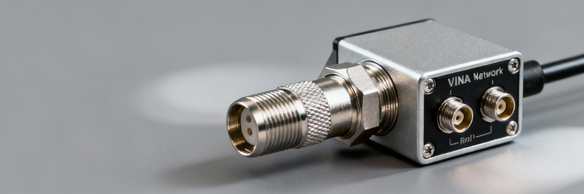
Point: The part is a NEX10 right‑angle plug family member intended for high‑frequency test and transceiver modules. Evidence: Typical family notes list series, gender and mounting style near the title block. Explanation: Confirm the part number string and series on the datasheet header, then note intended use (test jigs, board‑level RF feed) so you only apply relevant RF limits during design and procurement.
1.2 Datasheet sections & typical layout
Point: A connector datasheet follows a repeatable layout: electrical/RF specs, mechanical drawings, materials/finish, environmental parameters and assembly notes. Evidence: Measurement condition lines (e.g., “measured with 50 Ω system”, reference plane) appear above RF tables or graph captions. Explanation: Scan for RF graphs, table footnotes, and ECAD/STEP availability early—these items determine whether the datasheet contains usable RF test points and footprint files for layout import.
2 — Key RF Specs Explained (What to read, why it matters)
2.1 Frequency range, VSWR/Return Loss, & insertion loss
Point: Frequency range, VSWR (or S11/return loss) and insertion loss (S21) dictate link budget and matching. Evidence: Datasheets show either tabular passbands or swept plots with baseline conditions. Explanation: Translate VSWR to return loss for clarity (e.g., VSWR 1.5 ≈ 14 dB return loss) and flag insertion loss that erodes margin; use the plotted worst‑case at the highest frequency for acceptance criteria.
2.2 Impedance, isolation, and PIM / intermodulation
Point: Nominal impedance (usually 50 Ω), isolation between ports, and any PIM rating are critical for multi‑carrier systems. Evidence: The datasheet will state nominal Z and list isolation in dB or PIM in dBc with test tone levels. Explanation: Treat mismatch as a source of reflection; require ≤1.5 VSWR or equivalent return‑loss thresholds and set PIM thresholds (e.g., ≤‑150 dBc) per system spec to avoid degrading RX performance under high TX power.
3 — Mechanical & Environmental Specs That Affect RF Performance
3.1 Mechanical drawings, PCB footprint & mounting constraints
Point: Mechanical tolerances and the PCB land pattern affect impedance continuity and solder reliability. Evidence: Datasheet mechanical pages show recommended land patterns and clearances with mm or mil dimensions. Explanation: Import the STEP/ECAD model into your CAD, check right‑angle protrusion and keepout areas, and verify the footprint against your board stack and routing to prevent stray capacitance that shifts RF behavior.
3.2 Materials, plating, temperature range, and durability
Point: Conductor materials, insulator dielectric and plating change contact resistance, loss and PIM over life. Evidence: Material tables list contacts, dielectric type, plating (e.g., gold over nickel) and mating cycles. Explanation: Record finish and mating cycles for procurement and include contact plating and operating temperature limits in environmental tests to catch derating or PIM increases after thermal stress.
4 — How to Verify Compatibility & Validate Specs in the Lab
4.1 Cross-checking mating parts & system compatibility
Point: Confirm complementary part numbers, gender and the “measured mated” condition before trusting RF numbers. Evidence: Notes often specify whether performance was measured mated to a reference adapter or as a standalone. Explanation: Build a compatibility matrix (connector ↔ mating part ↔ cable ↔ system impedance) and reject combinations where the datasheet states measurements used adapters that differ from your target mating geometry.
4.2 Practical RF test checklist (what to measure and how)
Point: Key lab checks are S11 and S21 sweeps with VNA, plus PIM and thermal cycling as required. Evidence: Calibration and reference plane location are critical—datasheets note where measurements terminate. Explanation: Calibrate to the mating plane, capture S11 sweep across the full band, record insertion loss and run PIM tests under expected TX power; preserve margins by specifying acceptance criteria 1.5–2× stricter than datasheet minima.
5 — Quick Reference Checklist & Common Pitfalls
5.1 One-page procurement & design checklist
Point: A concise checklist ensures no spec is missed during review. Evidence: Standard items include part number, impedance, frequency, VSWR, insertion loss, PIM/power handling, footprint, ECAD files and RoHS notes. Explanation: Copy this checklist into your BOM and design review items so buyers and engineers verify electrical and mechanical compatibility before ordering prototypes.
5.2 Common misreads and how to avoid them
Point: Common errors include misreading measurement conditions, confusing dB and dBm, and assuming cable data applies to the connector. Evidence: Footnotes or “measured with adapter” notes are easy to overlook. Explanation: Annotate datasheet rows as “use for design”, “use for test” or “ignore for this project” and flag adaptor conditions so teams use consistent test baselines and avoid rework.
Summary
- Verify nominal impedance and frequency coverage first to ensure the connector fits your RF chain; include VSWR and insertion‑loss targets in layout rules and procurement notes for consistent performance.
- Check mechanical drawings and import STEP/ECAD files to validate footprint, right‑angle clearance, and solder land patterns before layout to avoid mechanical rework.
- Plan lab validation: VNA S11/S21 sweeps, PIM under realistic power, and thermal cycling; derive acceptance thresholds with margin beyond datasheet minima to cover assembly variability.
FAQ
How do I confirm 89S201-272N1 pin‑out and mating compatibility?
Check the datasheet header for the full part string and any listed complementary part numbers; cross‑reference the mechanical drawings and the “mating” note that indicates whether specs were measured mated. Build a small compatibility table mapping connector, mating part, and cable to system impedance.
What are the essential RF specs to extract from the 89S201-272N1 Datasheet before layout?
Extract nominal impedance, usable frequency band, VSWR/return loss curves, insertion loss at band edges, isolation, and any PIM or power‑handling notes. Use the worst‑case plotted values for acceptance criteria and ensure the VNA calibration plane matches the datasheet reference plane.
How should I set pass/fail criteria for connector tests referenced to the 89S201-272N1?
Derive acceptance limits by taking datasheet minimums and adding margin for assembly and measurement variability—typically require better VSWR and lower insertion loss than listed. Include PIM thresholds if the datasheet lists them, and validate after thermal cycling to capture derating effects.
- Technical Features of PMIC DC-DC Switching Regulator TPS54202DDCR
- STM32F030K6T6: A High-Performance Core Component for Embedded Systems
- APT50GH120B Datasheet Deep Dive: Specs, Ratings & Curves
- APT50GH120BSC20 Power Module: Latest Performance Report
- APT50GH120BD30 IGBT: How to Maximize Efficiency for EV Drive
- GTSM20N065: Latest 650V IGBT Test Report & Metrics
- CMSG120N013MDG Performance Report: Efficiency & Losses
- GTSM40N065D Technical Deep Dive: 650V IGBT + SiC SBD
- NOMC110-410UF SO-16: Live Stock & Price Report
- 1757255 MSTBA 5.08mm PCB: Step-by-Step Install & Solder
-
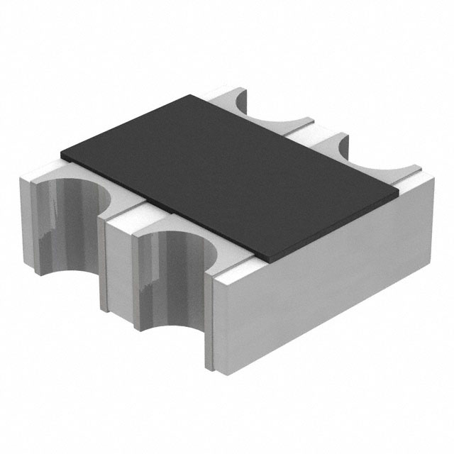 EXB-V4V120JVPanasonic Electronic ComponentsRES ARRAY 2 RES 12 OHM 0606
 -
 EXB-V4V473JVPanasonic Electronic ComponentsRES ARRAY 2 RES 47K OHM 0606
 -
 EXB-V4V823JVPanasonic Electronic ComponentsRES ARRAY 2 RES 82K OHM 0606
 -
 EXB-V4V151JVPanasonic Electronic ComponentsRES ARRAY 2 RES 150 OHM 0606
 -
 EXB-V4V181JVPanasonic Electronic ComponentsRES ARRAY 2 RES 180 OHM 0606
 -
 EXB-V4V331JVPanasonic Electronic ComponentsRES ARRAY 2 RES 330 OHM 0606
 -
 EXB-V4V152JVPanasonic Electronic ComponentsRES ARRAY 2 RES 1.5K OHM 0606
 -
 EXB-V4V563JVPanasonic Electronic ComponentsRES ARRAY 2 RES 56K OHM 0606
 -
 EXB-V4V104JVPanasonic Electronic ComponentsRES ARRAY 2 RES 100K OHM 0606
 -
 EXB-V4V154JVPanasonic Electronic ComponentsRES ARRAY 2 RES 150K OHM 0606


