-
- Contact Us
- Privacy Policy
- term and condition
- Cookies policy
59K101-271L5 datasheet: Complete electrical, RF specs
Measured and published specifications place the 59K101-271L5 in the DC–4 GHz class with a 50 Ω nominal impedance — key for high-frequency board-level designs. This article synthesizes the full electrical and RF specifications from the official datasheet and test reports, explains how to interpret them, and gives practical integration and test guidance. It draws the critical electrical specs and RF specs together so engineers can evaluate performance, procurement criteria, and bench test best practices before committing the part to a PCB layout.
1 — Quick product overview & intended applications (background introduction)

1.1 — Key identity and electrical envelope
59K101-271L5 datasheet: quick overview — Point: the part is a board-mount RF connector characterized for a 50 Ω system and a DC–4 GHz frequency envelope. Evidence: datasheet performance tables list nominal impedance 50 Ω and frequency range DC to 4 GHz. Explanation: this combination targets RF test jigs, board-level RF I/O, and sensor interfaces where low reflection and predictable insertion loss are required across the stated band.
1.2 — Mechanical summary & packaging notes
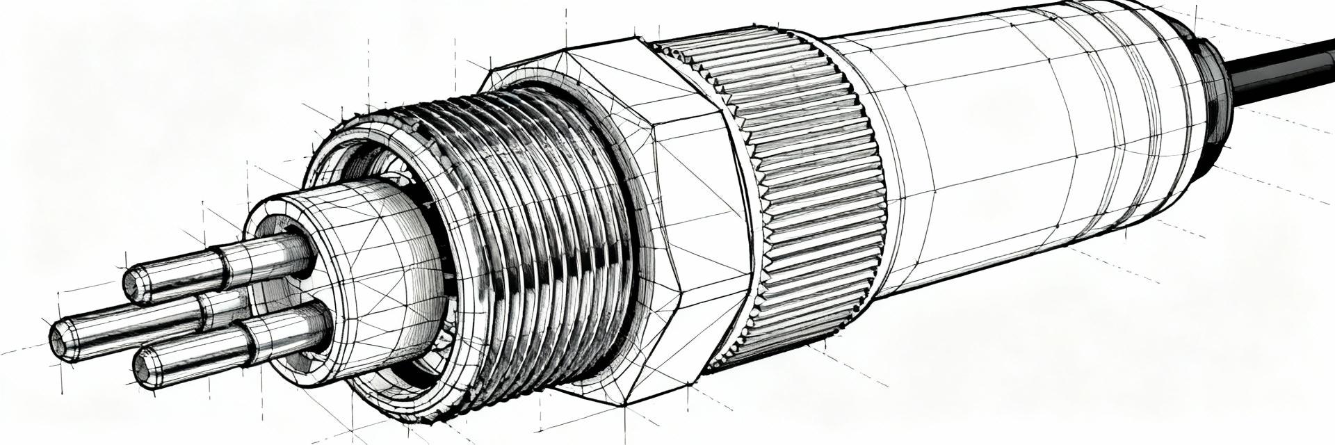
Point: mechanical highlights affect assembly and footprint selection. Evidence: typical mechanical items include connector gender, right-angle or vertical mounting, solder termination pads, and recommended footprint outlines in the datasheet. Explanation: engineers should extract the exact footprint drawing from the datasheet, verify pad dimensions against their PCB vendor rules, and prepare an annotated thumbnail or diagram of the connector footprint for DFM checks (avoid vendor logos in documentation).
2 — Electrical specs deep-dive (data analysis)
2.1 — DC and low-frequency electrical parameters
Point: DC parameters determine leakage, contact loss, and dielectric reliability. Evidence: documented values include insulation resistance ≥ 5 GΩ, contact resistance (center ≤ 6.0 mΩ, outer ≤ 2.0 mΩ), test voltage 500 V rms, and working voltage 335 V rms. Explanation: high insulation resistance limits leakage and noise coupling; low contact resistances minimize ohmic loss and heating at DC and low RF; voltage ratings inform isolation margins for mixed-signal boards. These electrical specs should be used in margin calculations for instrumentation and power-limited sensor lines.
| Parameter | Spec | Test condition / note |
|---|---|---|
| Insulation resistance | ≥ 5 GΩ | DC measurement, specified temperature |
| Contact resistance (center) | ≤ 6.0 mΩ | Initial, per contact |
| Contact resistance (outer) | ≤ 2.0 mΩ | Outer contact path |
| Test voltage | 500 V rms | Dielectric withstand |
| Working voltage | 335 V rms | Recommended continuous |
2.2 — Environmental & reliability test data
Point: reliability data define acceptance criteria for procurement and QC. Evidence: datasheet lists mating cycles, operating temperature range, shock/vibration results, and plating/contact materials. Explanation: report these values explicitly when specifying parts: mating durability for lifecycle planning, temperature extremes for environmental qualification, and plating details for corrosion resistance. A short procurement table is recommended for quick supplier QA checks.
| Parameter | Typical spec | Acceptance criteria |
|---|---|---|
| Mating cycles | Per datasheet (e.g., ≥ specified cycles) | Match or exceed system lifecycle |
| Temperature range | Per datasheet operating limits | Design margin ≥ 10°C beyond worst-case |
| Shock / vibration | Passed specified levels | Verify with board-level test |
| Plating / contact material | Specified precious metal / alloy | Confirm compatibility with solder and environment |
3 — RF specs & S-parameter guidance (data analysis)
3.1 — Frequency response and return loss / insertion loss
Point: RF numbers determine signal integrity across the stated band. Evidence: the connector is specified for 50 Ω; return loss ≥ 33 dB (DC–1 GHz), ≥ 30 dB (1–4 GHz); frequency range DC–4 GHz. Explanation: return loss thresholds translate to VSWR and allowable reflected power — ≥ 30 dB corresponds to VSWR ≈ 1.07, indicating excellent matching for antenna feeds and sensitive measurement points; insertion loss is typically low but must be plotted versus frequency for link-budget calculations.
| Parameter | Spec | Frequency range |
|---|---|---|
| Impedance | 50 Ω | DC–4 GHz |
| Return loss | ≥ 33 dB | DC–1 GHz |
| Return loss | ≥ 30 dB | 1–4 GHz |
| Insertion loss | Datasheet curve / measured S21 | Plot vs frequency |
3.2 — Measurement & S-parameter reporting best practices
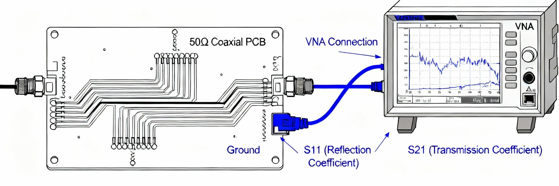
Point: consistent S-parameter reporting ensures reproducible comparison. Evidence: best practices include SOLT VNA calibration, fixture de-embedding, controlled test port conditions, and fixture loss compensation. Explanation: recommend publishing S11 magnitude & phase, S21 insertion loss, and Smith charts; provide raw CSV for each plotted curve and PNG for web figures. Document calibration method, connector mating torque, and de-embedding procedure for traceability.
4 — PCB footprint, soldering & integration procedures (method/guideline)
4.1 — Footprint, mounting recommendations and layout tips
Point: footprint and layout directly affect RF performance and assembly yield. Evidence: datasheet pad drawings specify pad size, keep-out zones, and anchor points. Explanation: critical tips include matching pad size to recommended land pattern, minimizing launch discontinuities with controlled microstrip transitions, placing ground stitching vias around the launch, and ensuring anchor pads are robust for mechanical stresses and reflow thermal cycles.
4.2 — Soldering, reflow profile and test-fixture installation
Point: soldering method and mechanical handling influence reliability and test repeatability. Evidence: datasheet provides recommended soldering method and reflow window when available; otherwise follow standard component profiles. Explanation: prefer reflow for production with verified profile; hand solder only for prototypes with inspection points. For bench RF testing, ensure correct torque, mating sequence, and fixture mounting to avoid biasing S-parameter measurements.
5 — Selection checklist, common failure modes & troubleshooting (case & action)
5.1 — Procurement / selection checklist
Point: a concise checklist reduces specification errors during procurement. Evidence: key items include required frequency range, impedance match, contact resistance limits, voltage rating, mating style, footprint compatibility, and environmental rating. Explanation: when reviewing the 59K101-271L5 datasheet, confirm each checklist item against system requirements and record acceptance criteria in the BOM entry to avoid late-stage mismatches.
5.2 — Common failure modes and fixes
Point: understanding failure modes speeds troubleshooting. Evidence: common issues include degraded return loss from poor mating or launch, intermittent contact from contamination, and solder joint cracks after thermal cycling. Explanation: fixes include reflowing or replacing solder joints, cleaning contact surfaces, improving ground stitching at the launch, and redoing VSWR sweeps after mechanical corrections; document tests (continuity, VNA sweep, visual inspection) in a troubleshooting flow.
Summary
Recap: the part delivers DC–4 GHz RF capability with a 50 Ω nominal impedance and clear electrical thresholds: insulation ≥ 5 GΩ, contact resistances ≤ 6.0 mΩ (center) and ≤ 2.0 mΩ (outer), and rated test/working voltages. Practical integration requires careful footprint verification, SOLT-calibrated S-parameter measurement with de-embedding, and procurement checks for mating durability and plating. Engineers should download the official datasheet and S-parameter files, verify footprint vs PCB rules, and run VNA verification with a calibrated fixture to confirm board-level performance for their use case.
Key summary
- Confirm 50 Ω and DC–4 GHz capability from the datasheet; use these electrical and RF specs for initial system compatibility checks and link-budget planning.
- Use the electrical specs table (insulation, contact resistance, voltage ratings) when defining procurement acceptance and test limits for incoming inspection.
- Follow SOLT calibration, fixture de-embedding, and publish S11/S21 (PNG + CSV) to validate RF specs against design requirements on the actual PCB.
FAQ
How should I verify the 59K101-271L5 datasheet S-parameters on my board?
Verify by performing a SOLT-calibrated VNA sweep with a de-embedded fixture that replicates the PCB launch. Capture S11 (magnitude and phase) and S21, save CSV for raw data, and compare return loss and insertion loss curves against the datasheet plots while documenting calibration and mating conditions.
What electrical specs matter most for low-noise sensor interfaces?
Insulation resistance and contact resistance are critical: high insulation (≥ 5 GΩ) reduces leakage and noise coupling; low contact resistance (
What are quick troubleshooting steps for poor return loss?
Start with visual inspection and continuity, clean contacts, verify correct mating and torque, reflow suspect solder joints, and re-run a VNA sweep. If issues persist, check ground stitching and launch geometry against the recommended footprint and improve de-embedding accuracy.
- Technical Features of PMIC DC-DC Switching Regulator TPS54202DDCR
- STM32F030K6T6: A High-Performance Core Component for Embedded Systems
- APT50GH120B Datasheet Deep Dive: Specs, Ratings & Curves
- APT50GH120BSC20 Power Module: Latest Performance Report
- APT50GH120BD30 IGBT: How to Maximize Efficiency for EV Drive
- GTSM20N065: Latest 650V IGBT Test Report & Metrics
- CMSG120N013MDG Performance Report: Efficiency & Losses
- GTSM40N065D Technical Deep Dive: 650V IGBT + SiC SBD
- NOMC110-410UF SO-16: Live Stock & Price Report
- 1757255 MSTBA 5.08mm PCB: Step-by-Step Install & Solder
-
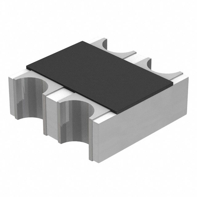 EXB-V4V120JVPanasonic Electronic ComponentsRES ARRAY 2 RES 12 OHM 0606
 -
 EXB-V4V473JVPanasonic Electronic ComponentsRES ARRAY 2 RES 47K OHM 0606
 -
 EXB-V4V823JVPanasonic Electronic ComponentsRES ARRAY 2 RES 82K OHM 0606
 -
 EXB-V4V151JVPanasonic Electronic ComponentsRES ARRAY 2 RES 150 OHM 0606
 -
 EXB-V4V181JVPanasonic Electronic ComponentsRES ARRAY 2 RES 180 OHM 0606
 -
 EXB-V4V331JVPanasonic Electronic ComponentsRES ARRAY 2 RES 330 OHM 0606
 -
 EXB-V4V152JVPanasonic Electronic ComponentsRES ARRAY 2 RES 1.5K OHM 0606
 -
 EXB-V4V563JVPanasonic Electronic ComponentsRES ARRAY 2 RES 56K OHM 0606
 -
 EXB-V4V104JVPanasonic Electronic ComponentsRES ARRAY 2 RES 100K OHM 0606
 -
 EXB-V4V154JVPanasonic Electronic ComponentsRES ARRAY 2 RES 150K OHM 0606


