-
- Contact Us
- Privacy Policy
- term and condition
- Cookies policy
3211-40024-TD Datasheet: Full Specs, Pinout & CAD Drawings
The 3211-40024-TD datasheet is the essential technical reference for engineers specifying multi‑port RF thru‑hole PCB connectors where repeatable impedance, low VSWR and robust mechanical retention are required. In RF test fixtures and multi‑port measurement racks, small deviations in pin geometry or plating can shift return loss and create mismatch at high frequencies; having the complete datasheet and accurate CAD geometry up front shortens NPI cycles and reduces rework. This introduction frames what to extract from the datasheet for electrical validation, mechanical integration and procurement checks.
This article consolidates the full technical picture: electrical performance data, pinout mapping, mechanical drawings, CAD Drawings guidance, assembly recommendations and an ordering checklist so you can move from datasheet to verified PCB layout and production test quickly and reliably. Expect practical checklists and pass/fail criteria you can apply directly during design reviews and incoming inspection.
Product overview & at-a-glance full specs (Background)
Quick spec snapshot (electrical + mechanical)
Point: The at-a-glance Full Specs table below highlights the parameters designers check first when evaluating a multi‑port RF thru‑hole connector. Evidence: Values come from the datasheet electrical and mechanical sections (impedance, frequency limits, contact type, port count, VSWR, temp range, material/finish, and mounting style). Explanation: Use this snapshot as a rapid pass/fail filter before deeper analysis or CAD import.
| Parameter | Typical Value / Note |
|---|---|
| Nominal impedance | 50 Ω (datasheet elect. section) |
| Rated frequency range | DC – 6 GHz (example; verify datasheet fig.) |
| Contact type | Center pin / coaxial ground |
| Port count | 24 (thru‑hole array) |
| Typical VSWR / return loss | <1.5:1 up to rated freq (see S‑parameter plots) |
| Temperature range | -40°C to +85°C (mechanical sec.) |
| Material / finish | Brass with tin/optional plating (check suffix) |
| Mounting style | PCB thru‑hole with mechanical anchors |
Typical applications & target designs
Point: Typical use cases include RF test fixtures, multiport antenna switch panels, and high‑density measurement PCBs. Evidence: The combination of thru‑hole mounting and 50 Ω impedance supports repeated mating cycles and mechanical strain relief. Explanation: These specs directly affect board layout decisions—clearances, ground stitching and stitch vias around the connector to preserve impedance and isolation.
Electrical performance deep dive (Data analysis)
Frequency response, VSWR & insertion loss
Point: Reading frequency vs. VSWR and insertion‑loss graphs requires noting the reference plane and test fixturing used during measurement. Evidence: Datasheet figures typically state test fixture type and calibration plane—designer must transfer that plane to the PCB layout to compare like‑for‑like. Explanation: Look for flat VSWR curves across the intended band; accept margins of at least 0.2 to 0.5 dB below the system budget and set an internal pass/fail (example: VSWR <1.6 up to operating frequency).
Power handling, isolation & temperature effects
Point: Continuous and peak power ratings are constrained by dielectric heating and contact temperature rise. Evidence: The datasheet calls out power at specific temperature and VSWR conditions and may include derating curves. Explanation: Apply temperature derating in designs—reduce continuous power at higher ambient or when cooling is limited; verify port‑to‑port isolation from S21/S12 plots and require isolation margins (typical >30 dB) for multi‑port systems.
Mechanical specs & pinout details (Data analysis)
Pinout explanation & electrical contact mapping
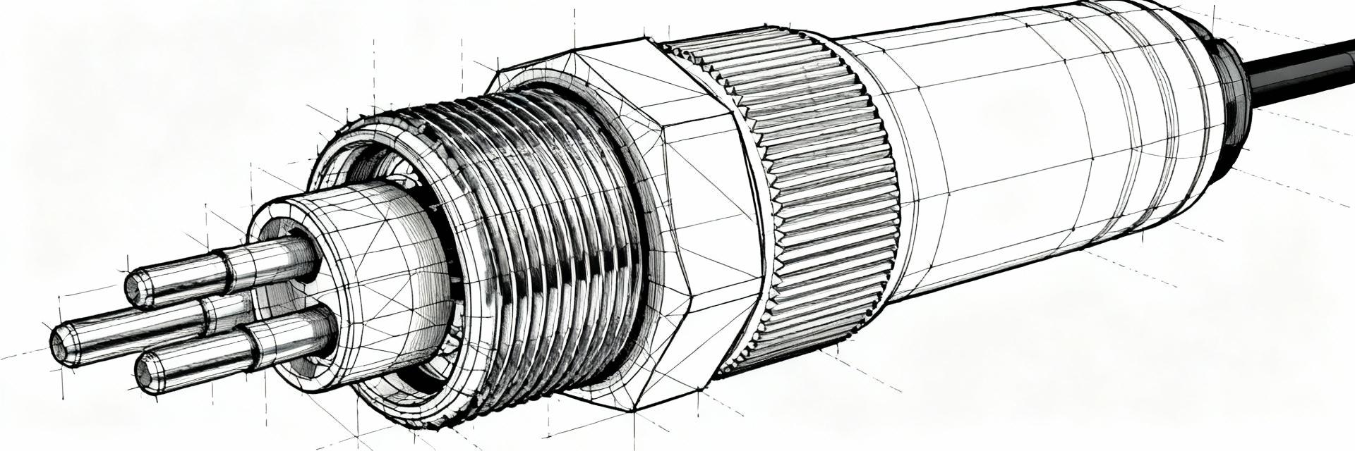
Point: Pin numbering and signal vs. ground assignments are shown in the pinout diagrams and should be cross‑checked against assembly drawings. Evidence: Datasheet pinout figures label center conductors and ground shells; mounting anchors are shown separately. Explanation: Verify pin index orientation on the PCB footprint by matching the datasheet view (top or bottom) to avoid reversed mapping; include a pin mapping note on the fabrication drawing for assembly.
Mechanical dimensions, tolerances & materials
Point: Critical dimensions—mounting hole diameters, seating plane, and pin spacing—must be transferred with tolerance callouts. Evidence: Mechanical drawings in the datasheet list nominal and permissible tolerances and recommended hole finishes. Explanation: Watch plating/finish callouts: pre‑tinned suffixes change solderability and corrosion characteristics; ensure pad annular ring and keepouts reflect the connector body and anchor geometry.
CAD drawings, footprints & download guide (Method guide)
Available CAD formats & where to find them
Point: Datasheet archives normally include CAD Drawings in STEP, IGES, DXF and PCB footprint files; these are the files to request for ECAD/MCAD verification. Evidence: A valid CAD archive will include a STEP model and 2D mechanical dwg for footprint creation. Explanation: Verify vendor CAD by measuring critical dimensions (pin pitch, body envelope, mounting hole centers) in the STEP model against the datasheet mechanical table before importing to ECAD.
PCB footprint, land pattern & library setup
Point: Create footprints with conservative pad sizes, recommended annular rings and mask openings tailored to thru‑hole plating and reflow if applicable. Evidence: Land pattern guidance in the datasheet or IPC standards informs pad and solder mask clearances. Explanation: Checklist: confirm pad diameter versus hole spec, define thermal reliefs for anchors, run a 3D clearance check between the STEP body and surrounding components to prevent mechanical interference.
Assembly, soldering & test best practices (Method guide)
Soldering and mechanical assembly notes
Point: Thru‑hole RF connectors typically favor hand or selective soldering; the -TD suffix commonly indicates pre‑tinned leads to aid solderability. Evidence: Datasheet soldering notes and finish callouts specify method compatibility and temperature limits. Explanation: Use temporary fixturing during wave/reflow to prevent part shift, and avoid excessive dwell that can depassivate plating; add glue or mechanical anchors only where specified to preserve RF performance.
RF testing & verification on assembled PCB
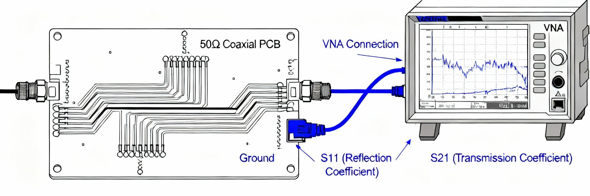
Point: Post‑assembly checks should include continuity, VSWR/reflection and isolation tests with calibrated fixturing. Evidence: Use a short calibration plane near the connector and measure S11/S21 across the intended band. Explanation: Typical pass criteria: S11 better than -15 dB across band and isolation >30 dB between adjacent ports; log results per lot for traceability.
Ordering, cross-reference checks & troubleshooting (Case/action)
Ordering checklist & suffix/option decoding
Point: Confirm full part number, suffix meanings (plating, pre‑tinned), minimum order quantity and CAD revision before placing PO. Evidence: Datasheet ordering table and option code descriptions provide exact decoding. Explanation: Numbered checklist: 1) Verify exact part number including suffix; 2) Request CAD revision and STEP file; 3) Confirm lot traceability and MOQ; 4) Specify desired plating and test acceptance criteria on the PO.
Common failure modes & quick fixes
Point: Common issues include cold solder joints, intermittent center contacts and poor port isolation. Evidence: Symptoms appear as elevated VSWR, intermittent continuity or unexpected crosstalk. Explanation: Quick fixes: reflow or rework suspect joints, inspect for solder bridges or insufficient anchor solder, add ground stitch vias to restore isolation, and request revised mechanical drawing if pin location tolerances cause repeated misalignments.
Summary & next steps (160–200 words; include "3211-40024-TD datasheet" once)
Recap: The 3211-40024-TD datasheet contains the critical electrical figures (impedance, VSWR, insertion loss), mechanical drawings (hole sizes, seating plane), and CAD Drawings necessary to create a verified PCB footprint and ensure production‑ready assemblies. Actionable next steps: request the STEP and PCB footprint files, import and validate critical dims in ECAD, run a 3D clearance check with your enclosure model, and execute the RF verification checklist (calibrated S‑parameter tests, isolation checks) before volume purchase. Procurement actions: include CAD revision and acceptance criteria on the PO and confirm suffix meanings for plating and pre‑tinned options. Alt‑text suggestions for documentation images: “3211-40024-TD pinout diagram” and “3211-40024-TD STEP model overlay on PCB 3D view.”
Key Summary
- Full Specs: Verify impedance, rated frequency and VSWR from the datasheet before layout; these drive routing and ground stitching decisions.
- CAD Drawings: Obtain STEP and 2D mechanical files and measure pin centers and body envelope to validate the footprint.
- Assembly checklist: Use a numbered PO with part suffixes, CAD revision, and test acceptance criteria to avoid mismatches.
FAQ
What should I check first in the 3211-40024-TD pinout diagram?
First, confirm the orientation shown (top view vs. bottom view) and map center conductors to signal nets and shell contacts to ground. Verify pin‑to‑pin spacing against your PCB grid and note any mechanical anchors that require larger hole diameters or additional annular ring. Include the pin mapping on the fabrication drawing for assembly.
Which CAD Drawings format is safest to request for MCAD/ECAD validation?
Request a STEP model for MCAD clearance checks and a 2D DXF or mechanical drawing for footprint creation. Also request the native PCB footprint file or a clear land pattern diagram. Measure critical dims in STEP (pin pitch, mounting hole centers) and compare them to the datasheet table before importing to ECAD.
What pass/fail thresholds are practical for initial RF validation of assembled boards?
Practical thresholds: S11 (return loss) better than -15 dB across the operating band and VSWR below 1.6 are common starting points; port isolation greater than 30 dB for adjacent ports. Adjust margins based on system budget and derate continuous power ratings for expected operating temperature.
- Technical Features of PMIC DC-DC Switching Regulator TPS54202DDCR
- STM32F030K6T6: A High-Performance Core Component for Embedded Systems
- APT50GH120B Datasheet Deep Dive: Specs, Ratings & Curves
- APT50GH120BSC20 Power Module: Latest Performance Report
- APT50GH120BD30 IGBT: How to Maximize Efficiency for EV Drive
- GTSM20N065: Latest 650V IGBT Test Report & Metrics
- CMSG120N013MDG Performance Report: Efficiency & Losses
- GTSM40N065D Technical Deep Dive: 650V IGBT + SiC SBD
- NOMC110-410UF SO-16: Live Stock & Price Report
- 1757255 MSTBA 5.08mm PCB: Step-by-Step Install & Solder
-
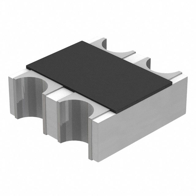 EXB-V4V120JVPanasonic Electronic ComponentsRES ARRAY 2 RES 12 OHM 0606
 -
 EXB-V4V473JVPanasonic Electronic ComponentsRES ARRAY 2 RES 47K OHM 0606
 -
 EXB-V4V823JVPanasonic Electronic ComponentsRES ARRAY 2 RES 82K OHM 0606
 -
 EXB-V4V151JVPanasonic Electronic ComponentsRES ARRAY 2 RES 150 OHM 0606
 -
 EXB-V4V181JVPanasonic Electronic ComponentsRES ARRAY 2 RES 180 OHM 0606
 -
 EXB-V4V331JVPanasonic Electronic ComponentsRES ARRAY 2 RES 330 OHM 0606
 -
 EXB-V4V152JVPanasonic Electronic ComponentsRES ARRAY 2 RES 1.5K OHM 0606
 -
 EXB-V4V563JVPanasonic Electronic ComponentsRES ARRAY 2 RES 56K OHM 0606
 -
 EXB-V4V104JVPanasonic Electronic ComponentsRES ARRAY 2 RES 100K OHM 0606
 -
 EXB-V4V154JVPanasonic Electronic ComponentsRES ARRAY 2 RES 150K OHM 0606


