-
- Contact Us
- Privacy Policy
- term and condition
- Cookies policy
6-1337482-0 RF SMB Connector Datasheet: Deep Dive Analysis
Point: A meta-review of typical SMB entries shows SMB-style 50 Ω coaxial connectors specified for DC–4 GHz with tight VSWR and compact PCB-mount variants tailored to space-constrained RF designs. Evidence: manufacturer datasheet fragments and quick-reference guides consistently list these baselines. Explanation: This article uses that context to extract the critical electrical, mechanical and integration details engineers need to specify, test, and deploy confidently; it references the 6-1337482-0 and the RF SMB connector family for clarity.
Point: Readers need an immediately actionable summary of what to verify on a datasheet. Evidence: common procurement and test failures stem from overlooked footprint, plating, or VSWR limits reported in the datasheet. Explanation: The introduction sets expectations: capture physical form, impedance/frequency envelope, S-parameters, and mechanical lifetime before specifying samples or production runs.
1 — Technical overview and connector family context (Background)
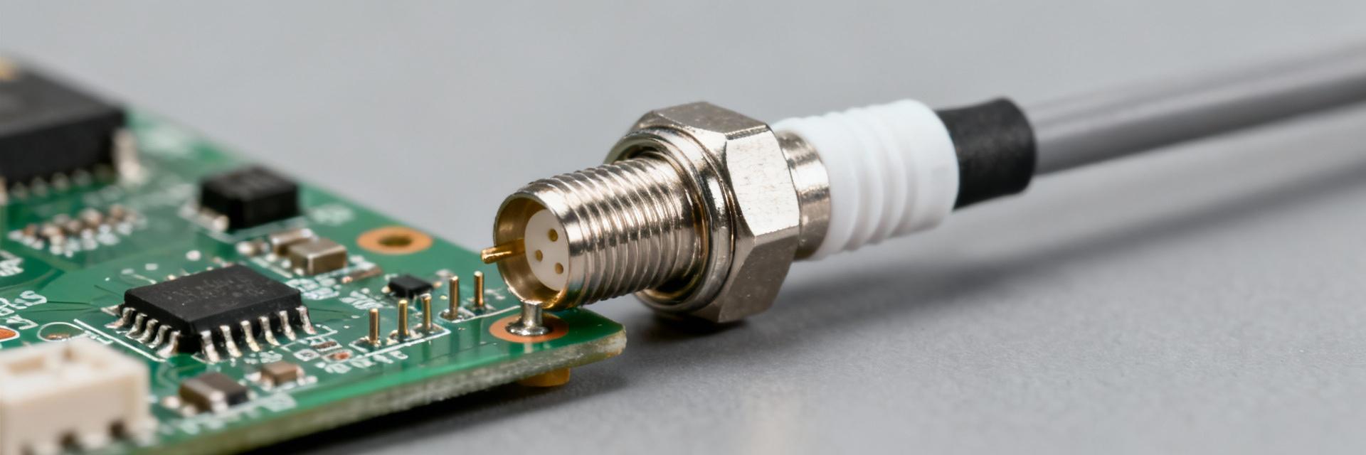
1.1 Connector type & form factor
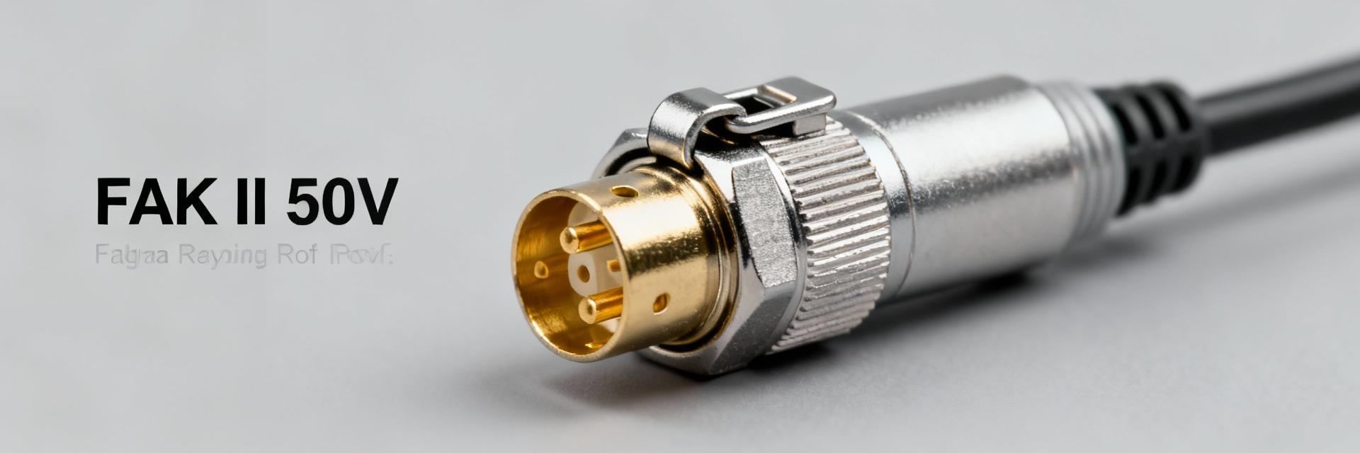
Point: The SMB style is a snap-on subminiature coaxial connector optimized for quick mating and compact footprints. Evidence: Typical SMB PCB jacks present short overall length, mated outer diameters near subminiature sizes, and either through-hole or surface-mount terminations. Explanation: For footprint planning, engineers should confirm whether the part is a jack or plug, straight or right-angle, and note the SMB PCB jack dimensions on the manufacturer drawing for clearance and assembly.
1.2 Electrical baseline: impedance, coupling, and typical frequency ranges
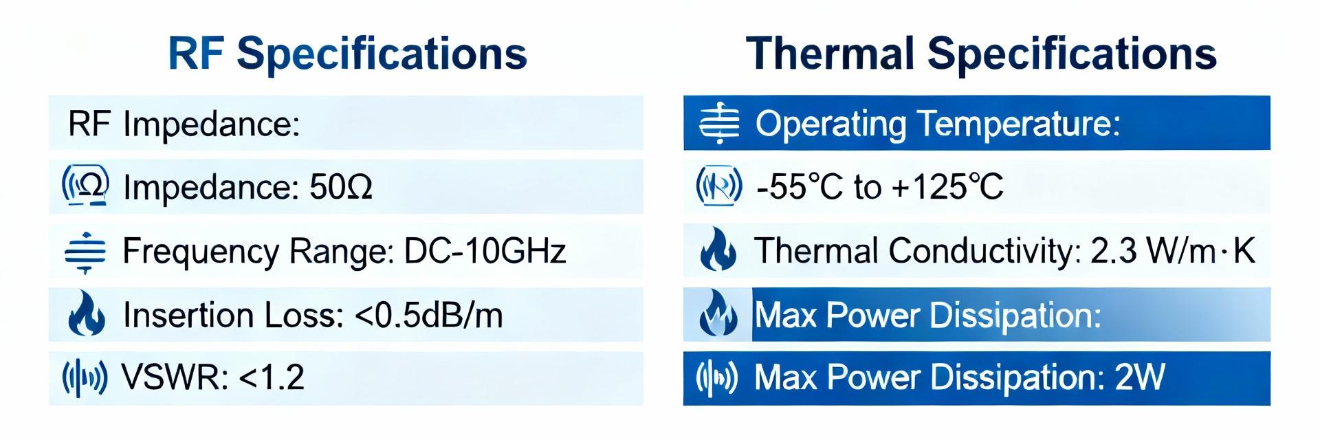
Point: SMB connectors are specified to 50 Ω nominal and commonly rated to DC–4 GHz as a baseline, with snap-on coupling impacting repeatability. Evidence: Datasheet fields to read first include impedance, frequency range, and VSWR/return loss across the band. Explanation: Comparing SMB to neighboring classes (e.g., SMA, SMC) shows trade-offs: SMB favors compactness and speed of mate/demate over the threaded coupling and marginally higher frequency ceiling of other classes.
2 — Datasheet parameter deep-dive (Data analysis)
2.1 Mechanical specifications: materials, finishes, tolerances
Point: The 6-1337482-0 datasheet will list body material, dielectric, center contact alloy, plating, torque or retention specs, and mating life. Evidence: Typical values include brass or beryllium copper bodies, PTFE dielectrics, gold-plated center contacts and nickel over brass shells with specified mating cycles. Explanation: Extract each field and compare to assembly and environment requirements—materials determine solderability, corrosion resistance, and wear under cyclic mating.
| Parameter | Datasheet value | Test condition | Pass/Fail threshold |
|---|---|---|---|
| Body material | Brass / Ni plating | As shipped | No visible corrosion |
| Center contact | BeCu / Au flash | Contact resistance test | <10 mΩ |
| Mating cycles | 500 cycles | Room temp, dry | No mechanical failure |
2.2 Electrical specifications: insertion loss, VSWR/return loss, power handling
Point: Key electrical parameters are insertion loss (S21), VSWR/return loss (S11), DC resistance, and power handling across the declared band. Evidence: Datasheets provide S-parameter points or curves, maximum insertion loss per frequency, and VSWR limits; test conditions often indicate temperature and fixture type. Explanation: Capture both typical and maximum values, note the test fixturing that can mask connector discontinuities, and flag any derating with temperature or frequency.
3 — Performance testing & validation (Data analysis / Method)
3.1 Recommended test setups and measurement methods
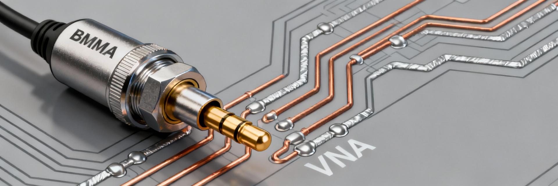
Point: Validation requires calibrated VNA measurement with appropriate fixtures and de-embedding; SOLT calibration to the connector interface is recommended. Evidence: Best practice uses short cables/fixtures, calibration standards at the connector plane and fixture de-embedding to remove board or adapter effects. Explanation: For PCB-mounted SMB, include a mate/demate sequence in test plans, sweep beyond the claimed band to observe resonances, and record fixture notes so test results are reproducible.
3.2 Typical acceptance criteria and troubleshooting signals
Point: Acceptance criteria should be defined from datasheet claims with margin—example VSWR <1.5 up to DC–4 GHz, insertion loss <0.2 dB at low GHz. Evidence: Common failure modes are solder joints, plating wear, or misalignment causing elevated return loss. Explanation: Troubleshoot with visual inspection, continuity checks, and swept return loss; isolate mechanical issues by swapping mating halves and verifying contact resistance under load.
4 — Design and PCB integration guidelines (Method)
4.1 PCB footprint, mechanical mounting and soldering recommendations
Point: Footprint guidance should come from the mechanical drawing: land pattern, hole size for through-hole, and solder fillet expectations. Evidence: Manufacturer mechanical drawings specify keepout, reference plane cutouts and recommended solder fillet heights for reliable joints. Explanation: For SMT SMBs use solder fillet acceptance criteria, avoid excessive reflow temperatures on plated contacts, and request sample reflow curves if contact plating or dielectric is temperature-sensitive.
4.2 Impedance control, grounding and RF layout best practices
Point: Controlled-impedance trace routing, reference plane continuity and ground via placement near the connector are essential to preserve VSWR. Evidence: Layout notes typically call for a continuous ground plane under the connector and multiple ground vias adjacent to mounting pads. Explanation: Maintain a solid reference plane up to the connector rear, minimize discontinuities, and ensure sufficient clearance to avoid stray capacitance that degrades return loss.
5 — Applications and selection criteria (Case)
5.1 Common system-level applications and environment suitability
Point: SMB variants like this part are common in compact RF modules, test jacks, short-run cable assemblies and handheld wireless devices. Evidence: Datasheets include environmental limits—operating temperature range, vibration and shock ratings—that determine suitability. Explanation: Confirm mechanical retention and plating for field devices where frequent mating occurs; for test environments, prioritize robust mating cycles and low insertion loss.
5.2 How to choose the right variant and alternatives
Point: A decision checklist helps select correct variant: required frequency, power handling, mating cycles, PCB space and retention type. Evidence: Substitutions must be checked for pinout, footprint, and equivalent electrical performance to avoid rework. Explanation: When substituting, compare mechanical drawings, S-parameter plots and mating instructions; request a sample for electrical validation to avoid surprises in production.
6 — Procurement, compliance and datasheet verification checklist (Action)
6.1 Datasheet verification checklist before purchase
Point: Procurement should verify part number, footprint drawing, electrical specs at required frequency, mechanical drawing, material/finish, mating instructions and packaging. Evidence: A concise verification table simplifies supplier responses and internal sign-off prior to ordering. Explanation: Capture each verified field against the manufacturer reference and test evidence; include a sample request clause so procurement secures validation parts for VNA testing before full buys—record this in the 6-1337482-0 datasheet pinout verification.
| Field | Verified value |
|---|---|
| Part number | Confirmed matches assembly |
| Footprint | Mechanical drawing matched |
| Electrical | VSWR / IL at required band |
6.2 Compliance, life-cycle and sourcing tips
Point: Confirm RoHS/REACH declarations, lot traceability and whether the part is current or superseded. Evidence: Manufacturers often publish qualification reports and change notices that affect long-term sourcing. Explanation: Procurement tactics include requesting samples, confirming lot traceability for automated assembly, and specifying packaging suitable for pick-and-place to reduce assembly risk and ensure consistent yield.
Summary
- Verify impedance, frequency and S-parameters on the manufacturer datasheet before specifying the 6-1337482-0 part for any 50 Ω RF path; validate with VNA measurement against claimed VSWR and insertion loss.
- Confirm mechanical drawings and SMB PCB jack dimensions for footprint, mounting and solder fillet expectations to prevent assembly failures and ensure repeatable performance in compact RF designs.
- Use a calibrated SOLT VNA setup with fixture de-embedding and a defined mate/demate protocol to reproduce datasheet results and catch plating or tolerance issues early.
FAQ
What should be checked first on the RF SMB connector datasheet?
Point: First check impedance, frequency range and VSWR/return loss. Evidence: These electrical fields determine RF compatibility and are commonly listed near the datasheet header. Explanation: Confirm these values against system requirements, and if margins are tight, request S-parameter data and physical samples for VNA validation prior to procurement.
How can engineers validate the 6-1337482-0 performance for production?
Point: Validate with calibrated VNA sweeps, fixture de-embedding and mate/demate cycles. Evidence: Acceptance criteria should map to datasheet claims with defined margins for VSWR and insertion loss. Explanation: Include mechanical inspections, contact resistance checks and environmental spot tests as part of incoming quality to ensure production units match validated samples.
- Technical Features of PMIC DC-DC Switching Regulator TPS54202DDCR
- STM32F030K6T6: A High-Performance Core Component for Embedded Systems
- APT50GH120B Datasheet Deep Dive: Specs, Ratings & Curves
- APT50GH120BSC20 Power Module: Latest Performance Report
- APT50GH120BD30 IGBT: How to Maximize Efficiency for EV Drive
- GTSM20N065: Latest 650V IGBT Test Report & Metrics
- CMSG120N013MDG Performance Report: Efficiency & Losses
- GTSM40N065D Technical Deep Dive: 650V IGBT + SiC SBD
- NOMC110-410UF SO-16: Live Stock & Price Report
- 1757255 MSTBA 5.08mm PCB: Step-by-Step Install & Solder
-
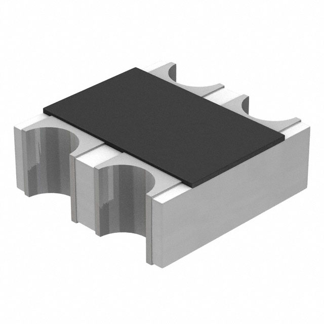 EXB-V4V120JVPanasonic Electronic ComponentsRES ARRAY 2 RES 12 OHM 0606
 -
 EXB-V4V473JVPanasonic Electronic ComponentsRES ARRAY 2 RES 47K OHM 0606
 -
 EXB-V4V823JVPanasonic Electronic ComponentsRES ARRAY 2 RES 82K OHM 0606
 -
 EXB-V4V151JVPanasonic Electronic ComponentsRES ARRAY 2 RES 150 OHM 0606
 -
 EXB-V4V181JVPanasonic Electronic ComponentsRES ARRAY 2 RES 180 OHM 0606
 -
 EXB-V4V331JVPanasonic Electronic ComponentsRES ARRAY 2 RES 330 OHM 0606
 -
 EXB-V4V152JVPanasonic Electronic ComponentsRES ARRAY 2 RES 1.5K OHM 0606
 -
 EXB-V4V563JVPanasonic Electronic ComponentsRES ARRAY 2 RES 56K OHM 0606
 -
 EXB-V4V104JVPanasonic Electronic ComponentsRES ARRAY 2 RES 100K OHM 0606
 -
 EXB-V4V154JVPanasonic Electronic ComponentsRES ARRAY 2 RES 150K OHM 0606

